SG55327 Ver la hoja de datos (PDF) - Microsemi Corporation
Número de pieza
componentes Descripción
Fabricante
SG55327 Datasheet PDF : 3 Pages
| |||
SG55327/SG75327
ELECTRICAL CHARACTERIZATICS (continued)
Parameter
Static Section (continued)
Supply Current (ICC(OFF))
From V
CC1
From VCC2
Supply Current (ICC(ON))
From VCC1
From VCC2
Test Conditions
SG55327
SG75327
Units
Min. Typ. Max. Min. Typ. Max.
All outputs off, all inputs at 5V, TA = 25°C
One output on, ISOURCE = -50mA,
V
COL
=
6V,
T
A
=
25°C
7.0 10
13 20
8.0 12
36 55
10
7.0 20 mA
13
mA
12
8.0 55 mA
36
mA
Parameter
To (output)
Test Conditions
Dynamic Section (Note 5)
Propagation Delay, Low to High (TPLH)
Propagation Delay, High to Low (TPHL)
Transition Time, Low to High (TTLH)
Transition Time, High to Low (TTHL)
High-Level Output Voltage (VOH)
(Note 6)
Coll. W, Z or X, Y
Coll. W, Z or X, Y
W, X, Y, or Z
W, X, Y, or Z
Coll. W, Z or X, Y
V
S
=
V
CC2
=
15V,
R
L
=
24Ω
VS = VCC2 = 15V, RL = 24Ω
VCOL = VCC2 = 20V, RL = 100Ω
V
COL
=
V
CC2
=
20V,
R
L
=
100Ω
VS = VCC2 = 24V, RL = 47Ω,
ISINK ≈ 500mA
Note 4. Under these conditions, not more than one output is to be on any one time.
Note 5. Unless otherwise specified, VCC1 = 5V, CL = 25pF, and TA = 25°C.
Note 6. Guaranteed but not tested.
SG55327/75327 Units
Min. Typ. Max.
35 55 ns
30 55 ns
30
ns
10
ns
VS–25
mV
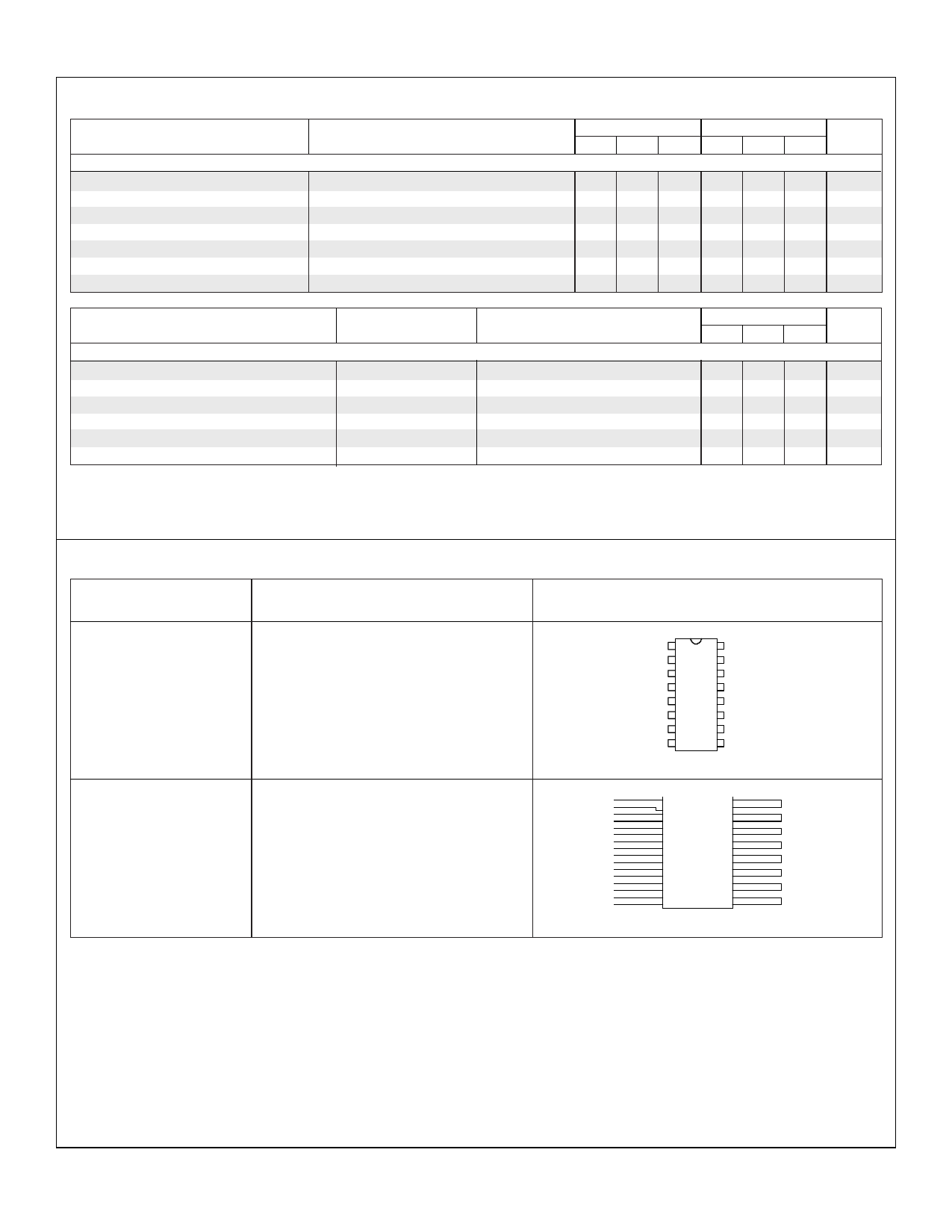
CONNECTION DIAGRAMS & ORDERING INFORMATION (See Notes Below)
Package
Part No.
Ambient
Temperature Range
Connection Diagram
16-PIN CERAMIC DIP
J - PACKAGE
16-PIN PLASTIC DIP
N - PACKAGE
SG55327J/883B
SG55327J
SG75327J
-55°C to 125°C
-55°C to 125°C
0°C to 70°C
SG75327N
0°C to 70°C
VCC2
1
16 COLLECTORS W, Z
W
2
15 Z
A
3
14
D
NODE R
4
13
S
RINT
5
12
VCC1
B
6
11
C
X
7
10
Y
GND (Note 2) 8
9 COLLECTORS X, Y
16-PIN CERAMIC
FLAT PACK
F - PACKAGE
SG55327F/883B -55°C to 125°C
SG55327F
-55°C to 125°C
VCC2
W
A
NODE R
RINT
B
X
GND
1
16
2
15
3
14
4
13
5
12
6
11
7
10
8
9
COLL. W, Z
Z
D
S
VCC1
C
Y
COLL. X, Y
Note 1. All packages are viewed from the top.
Note 2. Pin 8 is in electrical contact with the metal base.
4/90 Rev 1.2 7/96
Copyright © 1994
3
LINFINITY Microelectronics Inc.
11861 Western Avenue ∞ Garden Grove, CA 92841
(714) 898-8121 ∞ FAX: (714) 893-2570
Share Link: 