SCAN18245T Ver la hoja de datos (PDF) - Fairchild Semiconductor
Número de pieza
componentes Descripción
Fabricante
SCAN18245T Datasheet PDF : 11 Pages
| |||
Truth Table
Inputs
G1 DIR1
L
L
L
L
L
H
L
H
H
X
H= HIGH Voltage Level
L= LOW Voltage Level
A1 (0–8)
B1 (0–8)
H
←
H
L
←
L
H
→
H
L
→
L
Z
Z
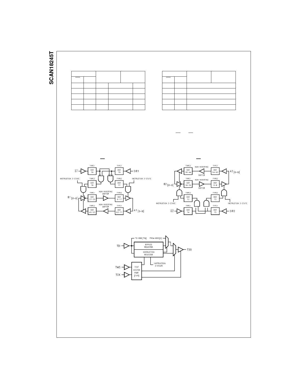
Functional Description
The SCAN18245 consists of two sets of nine non-inverting
bidirectional buffers with 3-STATE outputs and is intended
for bus-oriented applications. Direction pins (DIR1 and
DIR2) LOW enables data from B Ports to A Ports, when
Block Diagrams
Inputs
G2 DIR2
L
L
L
L
L
H
L
H
H
X
X= Immaterial
Z= High Impedance
A2 (0–8)
B2 (0–8)
H
←
H
L
←
L
H
→
H
L
→
L
Z
Z
HIGH enables data from A Ports to B Ports. The Output
Enable pins (G1 and G2) when HIGH disables both A and
B Ports by placing them in a high impedance condition.
A1, B1, G1 and DIR1
A2, B2, G2 and DIR2
Note: BSR stands for Boundary Scan Register.
Note: BSR stands for Boundary Scan Register.
Tap Controller
www.fairchildsemi.com
2
Share Link: 