RS56L-PCI Ver la hoja de datos (PDF) - Unspecified
Número de pieza
componentes Descripción
Fabricante
RS56L-PCI Datasheet PDF : 12 Pages
| |||
+RVW6RIWZDUH3URFHVVHG9
.IOH[™0RGHP'HYLFH)DPLO\IRU0RELOH$SSOLFDWLRQV
56/3&,
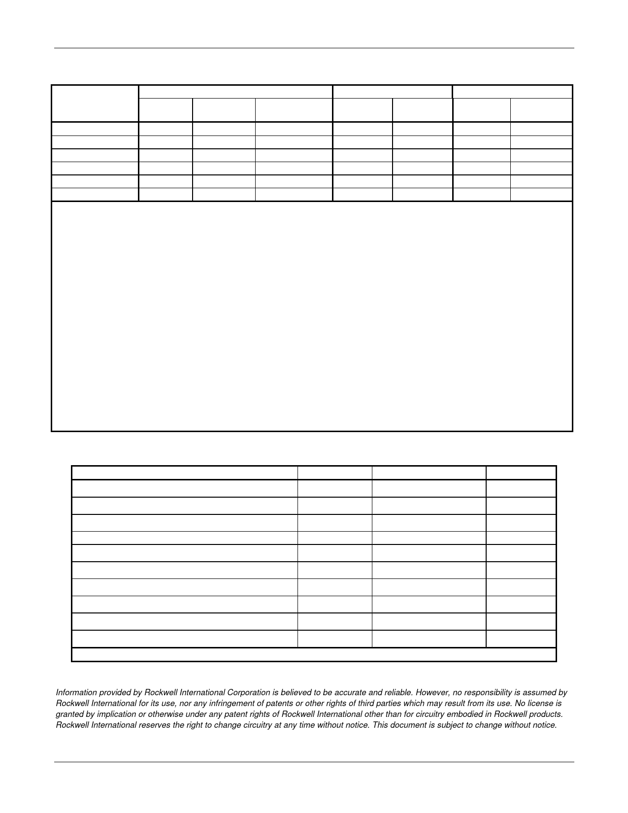
Table 4. Current and Power Requirements
Conditions
Current
Power
Device State (Dx)
and Bus State (Bx)
PCI Bus
Power
PCI Clock
(PCICLK)
Line
Connection
Typical
Maximum
Typical
Maximum
Current (mA) Current (mA) Power (mW) Power (mW)
D0, B0
On
Running
Yes
33
36
109
130
D0, B0
On
Running
No
22
24
73
86
D3, B0
On
Running
No
22
24
73
86
D3, B1
On
Running
No
22
24
73
86
D3, B2, B3 (D3 hot)
On
Stopped
No
2.1
3.2
6.9
11.5
D3, B3 (D3 cold)
Off
Stopped
No
<1
1
<3.3
3.6
Notes:
Operating voltage: VDD = +3.3V ± 0.3V.
Test conditions: VDD = +3.3 VDC for typical values; VDD = +3.6 VDC for maximum values.
For all modes, +3.3V is supplied to modem.
Definitions:
PCI Bus Power
On: PCI Bus +5V and +3.3V on (modem normally powered by +3.3V from PCI Bus +3.3V
or regulated down from PCI Bus +5V); PCIRST# not asserted.
Off: PCI Bus +5V and +3.3V off (modem normally powered by +3.3V from Vaux or Vpci); PCIRST# asserted.
PCI Clock (PCICLK)
Running: PCI Bus signal PCICLK running;
Stopped: PCI Bus signal PCICLK stopped (off).
Line connection:
Yes: Off-hook, IA powered.
No: On-hook, IA powered down.
Device States:
D3: Low power state. Suspend state can change the system power state; the resulting power state depends
on the system architecture (OS, BIOS, hardware) and system configuration (i.e., other PCI installed cards).
D0: Full power state.
Device and Bus States: D0, B0: Any PCI transaction, PCICLK running, VCC present.
D3, B1: No PCI Bus transactions, PCICLK running, VCC present.
D3, B2, B3: No PCI transactions, PCICLK stopped, VCC may be present.
D3, B3: No PCI transactions, PCICLK stopped, no VCC.
Refer to the PCI Bus Power Management Interface Specification for additional information.
Table 5. Absolute Maximum Ratings
Supply Voltage
Parameter
Input Voltage
Operating Temperature Range
Storage Temperature Range
Analog Inputs
Voltage Applied to Outputs in High Impedance (Off) State
DC Input Clamp Current
DC Output Clamp Current
Static Discharge Voltage (25°C)
Latch-up Current (25°C)
* VIO = +3.3V ± 0.3V or +5.0V ± 5%
Symbol
VDD
VIN
TA
TSTG
VIN
VHZ
IIK
IOK
VESD
ITRIG
Limits
-0.5 to +4.0
-0.5 to (VIO +0.5)*
-0 to +70
-55 to +125
-0.3 to (VAA + 0.5)
-0.5 to (VIO +0.5)*
±20
±20
±2500
±400
Units
V
V
°C
°C
V
V
mA
mA
V
mA
Information provided by Rockwell International Corporation is believed to be accurate and reliable. However, no responsibility is assumed by
Rockwell International for its use, nor any infringement of patents or other rights of third parties which may result from its use. No license is
granted by implication or otherwise under any patent rights of Rockwell International other than for circuitry embodied in Rockwell products.
Rockwell International reserves the right to change circuitry at any time without notice. This document is subject to change without notice.
0'
Share Link: 