RMPA0951AT Ver la hoja de datos (PDF) - Fairchild Semiconductor
Número de pieza
componentes Descripción
Fabricante
RMPA0951AT Datasheet PDF : 11 Pages
| |||
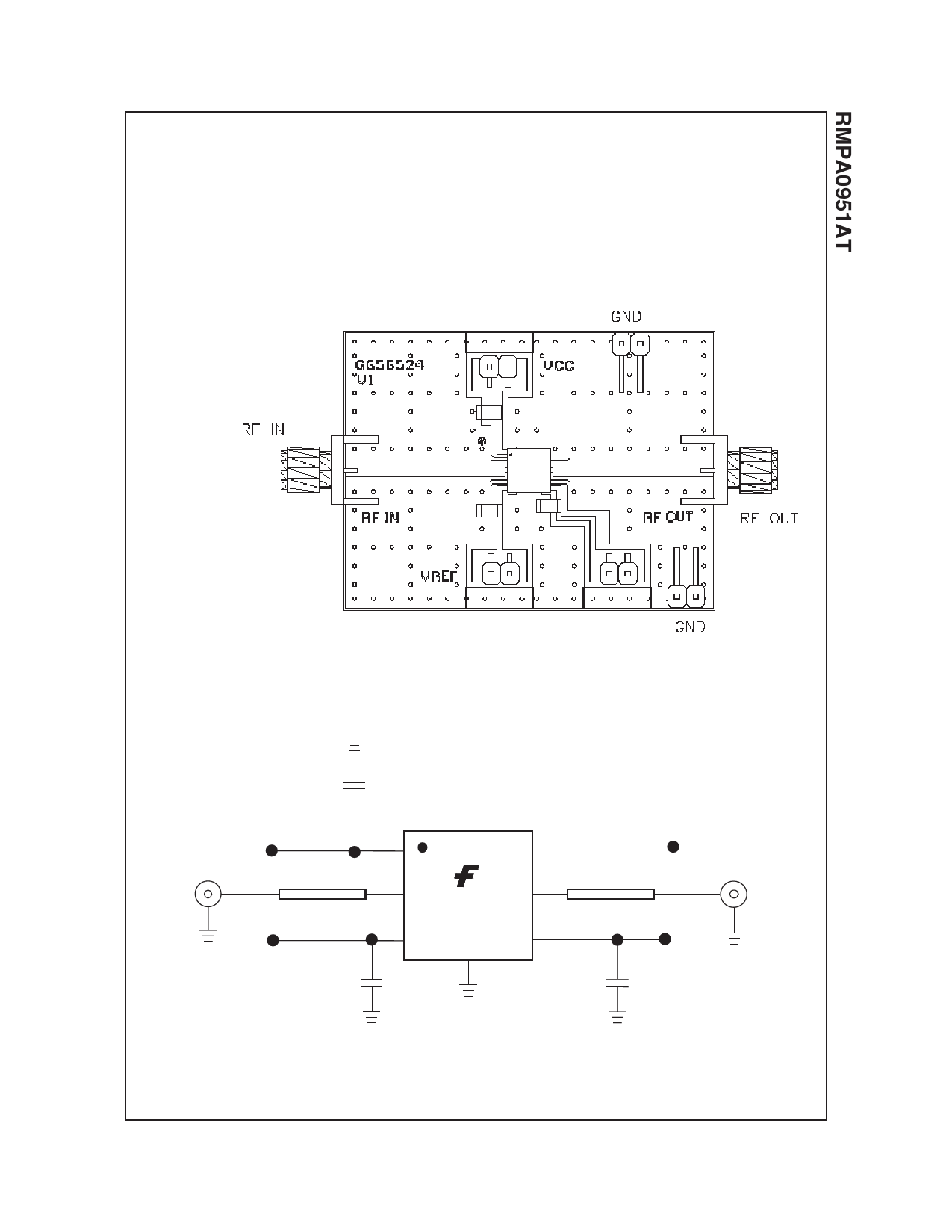
With device marking oriented right side up, RF IN is on the left and RF OUT is on the right.
Vcc = +3.4V nominal. Vref = +3.0V nominal to obtain Iccq = 80 mA. Operation at lower or higher quiescent currents can be
achieved by decreasing or increasing Vref voltage relative to +3.0V.
First ground the PCB (GND terminal) and apply +3.4V to the collector supply terminals (Vcc1, Vcc2). Next apply +3.0V to
the reference supply (Vref terminal). Quiescent collector current with no RF applied will be about 80 mA. Reference supply
current with or without RF applied will be about 15 mA. When turning amplifier off, reverse power supply sequence.
Apply -20dBm RF input power at Cellular frequency (824-849 MHz). After making any initial small signal measurements at
this drive level, input power may be increased up to a maximum of +7dBm for large signal, analog (AMPS) or digital CDMA
measurements. Do not exceed +7dBm input power.
Vcc1
PCB Specifications:
Material: Rogers R04003
Dimensions: 2.0"x1.5"x0.032"
Metallization: 1/2 oz
Copper Cladding
Vref
Vcc2
Figure 3. Evaluation Board Layout and Instructions
PCB Schematic
Note: Addition of C3 bypass
capacitor on Vref pin
recommended to minimize
Rx band noise
C1*
3.3 µF
SMA1
RF IN
Vcc1
Vref
50Ω TRL
C3*
1000 pF
1
6
N/C
2
5
RMPA0951AT
50Ω TRL
3
4
Vcc2
7 (package base)
C2*
3.3 µF
SMA2
RF OUT
* Minimum bypass capacitance recommended for best linearity/low-noise performance.
Figure 4. Evaluation Board Schematic
©2004 Fairchild Semiconductor Corporation
RMPA0951AT Rev. D
Share Link: 