RMBA19500 Ver la hoja de datos (PDF) - Fairchild Semiconductor
Número de pieza
componentes Descripción
Fabricante
RMBA19500 Datasheet PDF : 7 Pages
| |||
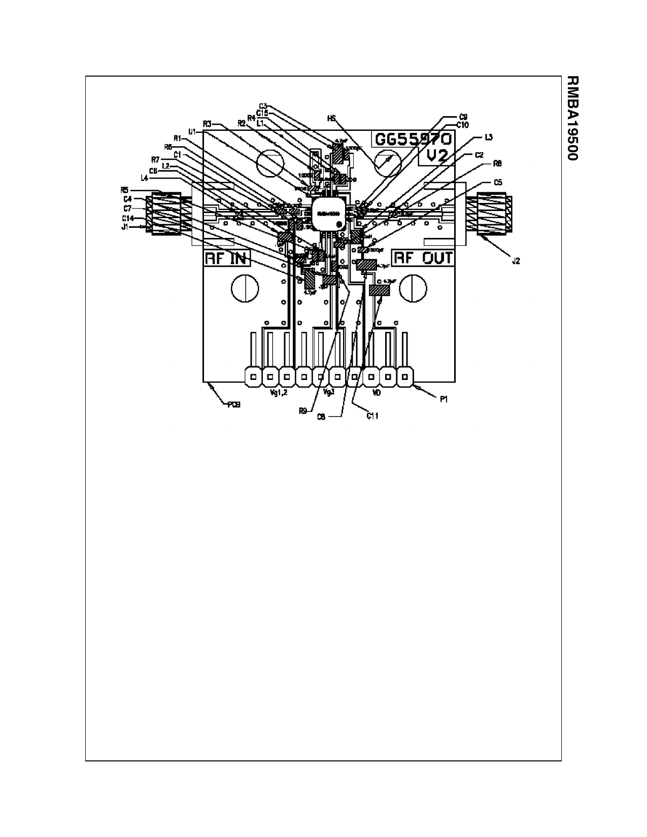
Figure 4. Layout of Test Evaluation Board (RMBA19500-TD, G655971)
Test Procedure for the Evaluation Board (RMBA19500-TB)
CAUTION: LOSS OF GATE VOLTAGES (Vg1, Vg2,
Vg3) WHILE CORRESPONDING DRAIN VOLTAGES
(Vdd) ARE PRESENT CAN DAMAGE THE AMPLIFIER.
The following sequence must be followed to properly test
the amplifier. (It is necessary to add a fan to provide air
cooling across the heat sink of RMBA19500.)
Step 1: Turn off RF input power.
Step 2: Use GND terminal of the evaluation board for the
ground of the DC supplies. Set Vgg1, Vgg2 and Vgg3 to
-3V (pinch-off).
Step 3: Slowly apply drain supply voltages of +7V to the
board terminal Vdd ensuring that there is no short.
Step 4: Adjust Vgg12 up from -3V until the drain current
(with no RF applied) increases to Idq12 as per supplied
result sheet. Then adjust Vgg3 until the total drain current
becomes equal to the sum of Idq12 and Idq3.
Step 5: After the bias condition is established, RF input
signal may now be applied at the appropriate frequency
band and appropriate power level.
Step 6: Follow turn-off sequence of:
(i) Turn off RF Input Power
(ii) Turn down and off drain voltage Vdd.
(iii) Turn down and off gate voltages Vgg1, Vgg 2 and
Vgg3.
©2003 Fairchild Semiconductor Corporation
RMBA19500 Rev. C
Share Link: 