RB-TA3020 Ver la hoja de datos (PDF) - Tripath Technology Inc.
Número de pieza
componentes Descripción
Fabricante
RB-TA3020
Tripath Technology Inc.

RB-TA3020 Datasheet PDF : 20 Pages
| |||
Tripath Technology, Inc. - Technical Information
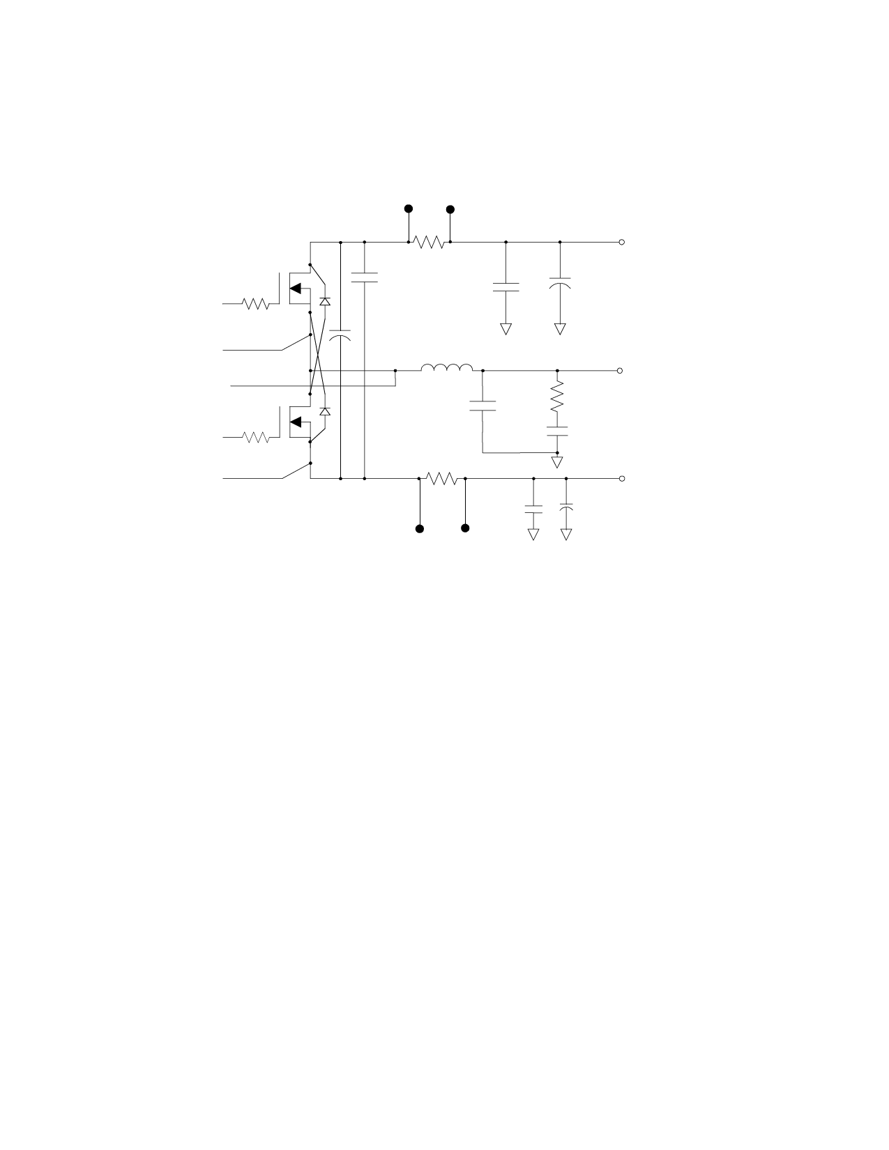
Output Section
The output section includes the gate resistors, output diodes, FETs, output filters, the previously
mentioned OVERCURRENT sense resistors, clamping diodes, a Zobel Network, and various bypass
capacitors.
M100/200
HO
R113/213
5.6 Ω
HOCOM
FBKOUT
M101/201
LO
R114/214
5.6 Ω
LOCOM
OCSHN
R115/215
0.01 Ω
OCSHP
C105/205
0.1uF, 250V
D106/206
MUR120
C106/206
0.1uF, 100V
C113/223
33uF, 160V
L100/200
11.3uH
D107/207
MUR120
C108/208
0.22uF, 100V
R116/216
0.01 Ω
OCSLP
C110/210
0.1uF, 100V
OCSLN
VPP
+
C7
330uF, 63V
OUT
R117/217
33 Ω/2W
C109/209
0.1uF, 100V
VNN
+ C6
330uF, 63V
Figure 8
The gate resistors (labeled R113, R213, R114, and R214 in Figure 8 and the attached schematic) are
used to control MOSFET switching rise/fall times and thereby minimize voltage overshoots. They also
dissipate a portion of the power resulting from moving the gate charge each time the MOSFET is
switched. If RG is too small, excessive heat can be generated in the driver. Large gate resistors lead to
slower gate transitions resulting in longer rise/fall times and thus requiring a larger BBM setting. Tripath
recommends using an RG of 5.6Ω when the Qg is greater than 70nC and RG of 10Ω when the gate charge
(Qg) of the output FET is less than 70nC.
The output FETs (M100, M101, M200 and M201) provide the switching function required of a Class-T
design. They are driven directly by the TA3020 through the gate resistors. The devices used on the
reference board are ST STW34NB20 MOSFETs. The TA3020 data sheet contains information on output
FET selection as well as Tripath application notes “FETs – Selection and Efficiency” and “Designing with
Switching
Amplifiers
for
Performance
and
Reliability”.
The bypass capacitors C105/C205 and C113/c213 are critical to the reduction of ringing on the outputs of
the FETs. These parts are placed as closely as possible to the leads of the FETs, and the leads of the
capacitors themselves are as short as practical. Their values will not change with different output FETs.
The output diodes D106/D107/D206/D207 are also critical to the reduction of ringing on the outputs of the
FETs. They shunt the inductive energy if the output exceeds VPP or goes below VNN. The proper
connection of these diodes are “drain to drain” and “source to source” as shown in the schematic
diagrams.
The output filters L100/C108 and L200/C208 are the low-pass filters that recover the analog audio signal.
One of the benefits of the Class-T design is the ability to use output filters with relatively high cutoff
frequencies. This greatly reduces the speaker interactions that can occur with the use of lower-frequency
filters common in Class-D designs. Also, the higher-frequency operation means that the filter can be of a
lower order (simpler and less costly).
8
RB-TA3020, Rev. 3.0/03.02
Share Link: