RB-TA3020-2 Ver la hoja de datos (PDF) - Tripath Technology Inc.
Número de pieza
componentes Descripción
Fabricante
RB-TA3020-2
Tripath Technology Inc.

RB-TA3020-2 Datasheet PDF : 20 Pages
| |||
Tripath Technology, Inc. - Technical Information
28V (-1 VERSION)
45V (-2 VERSION)
28V (-1 VERSION)
45V (-2 VERSION)
10V
HEATSINK
M100
M101
M201
VPP
PGND
VNN
VN10
M200
-+
OUT1
GND1
Ch1
Offset
AGND
IN1
AGND
V5
TA3020
HMUTE LED
GND2
OUT2
AGND
IN2
Ch2
Offset
BBM1
BBM0
MUTE
AUDIO
SOURCE
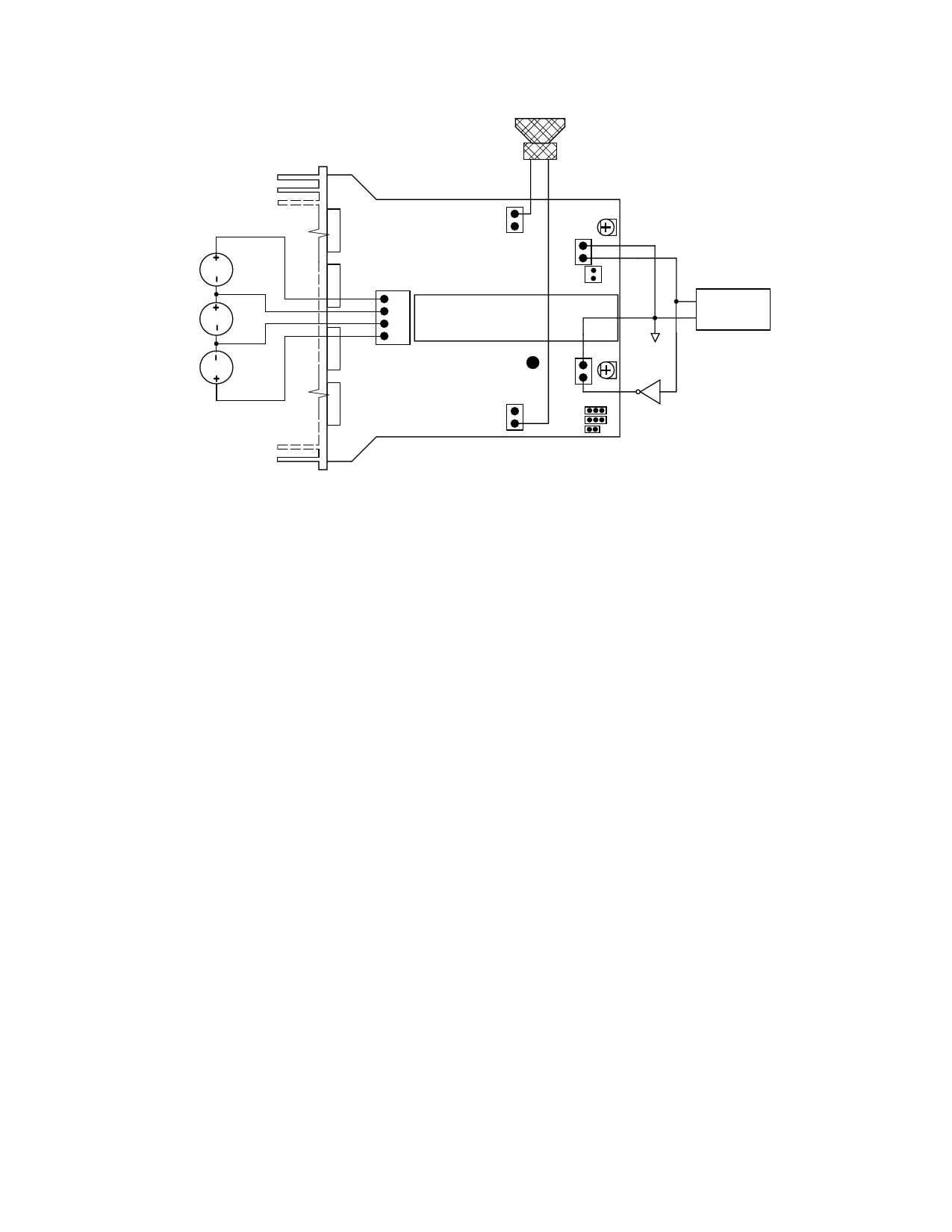
Figure 9
Circuit Board Layout
The TA3020 is a power (high current) amplifier that operates at relatively high switching frequencies.
The output of the amplifier switches between VPP and VNN at high speeds while driving large
currents. This high-frequency digital signal is passed through an LC low-pass filter to recover the
amplified audio signal. Since the amplifier must drive the inductive LC output filter and speaker loads,
the amplifier outputs can be pulled above the supply voltage and below ground by the energy in the
output inductance. To avoid subjecting the TA3020 to potentially damaging voltage stress, it is critical
to have a good printed circuit board layout. It is recommended that Tripath’s layout and application
circuit be used for all applications and only be deviated from after careful analysis of the effects of any
changes. Please refer to the TA3020 evaluation board document, EB-TA3020, available on the
Tripath website, at www.tripath.com.
The following components are important to place near either their associated TA3020 or output
MOSFET pins. The recommendations are ranked in order of layout importance, either for proper
device operation or performance considerations. The component designators, referred to, are for
channel 1 of the RB-TA3020.
- The capacitors, CHBR (C105/C113), provide high frequency bypassing of the amplifier power
supplies and will serve to reduce spikes across the supply rails. Please note that both
mosfet half-bridges must be decoupled separately. In addition, the voltage rating for CHBR
should be at least 150V as this capacitor is exposed to the full supply range, VPP-VNN.
- DO (D106/D107) are also critical to the reduction of ringing on the outputs of the FETs.
They shunt the inductive energy if the output exceeds VPP or goes below VNN. The
proper connection of these diodes are “drain to drain” and “source to source” as shown in
the schematic diagrams. These diodes have a 200V rating.
- CFB (C107) removes very high frequency components from the amplifier feedback signals
and lowers the output switching frequency by delaying the feedback signals. In addition,
the value of CFB is different for channel 1 and channel 2 to keep the average switching
frequency difference greater than 40kHz. This minimizes in-band audio noise. Locate
these capacitors as close to their respective TA3020 pin as possible.
10
RB-TA3020, Rev. 3.0/03.02
Share Link: