MGA-87563(1999) Ver la hoja de datos (PDF) - HP => Agilent Technologies
Número de pieza
componentes Descripción
Fabricante
MGA-87563 Datasheet PDF : 8 Pages
| |||
6
between the noise figure obtain-
able with a conjugate power
match at the input and NFo is only
about 0.2 dB.
Output Matching
The output of the MGA-87563 is
matched internally to 50 Ω above
1.8 GHz. The use of a conjugate
matching circuit, such as a simple
series inductor, can increase the
gain considerably at lower
frequencies. Matching the output
will not affect the noise figure.
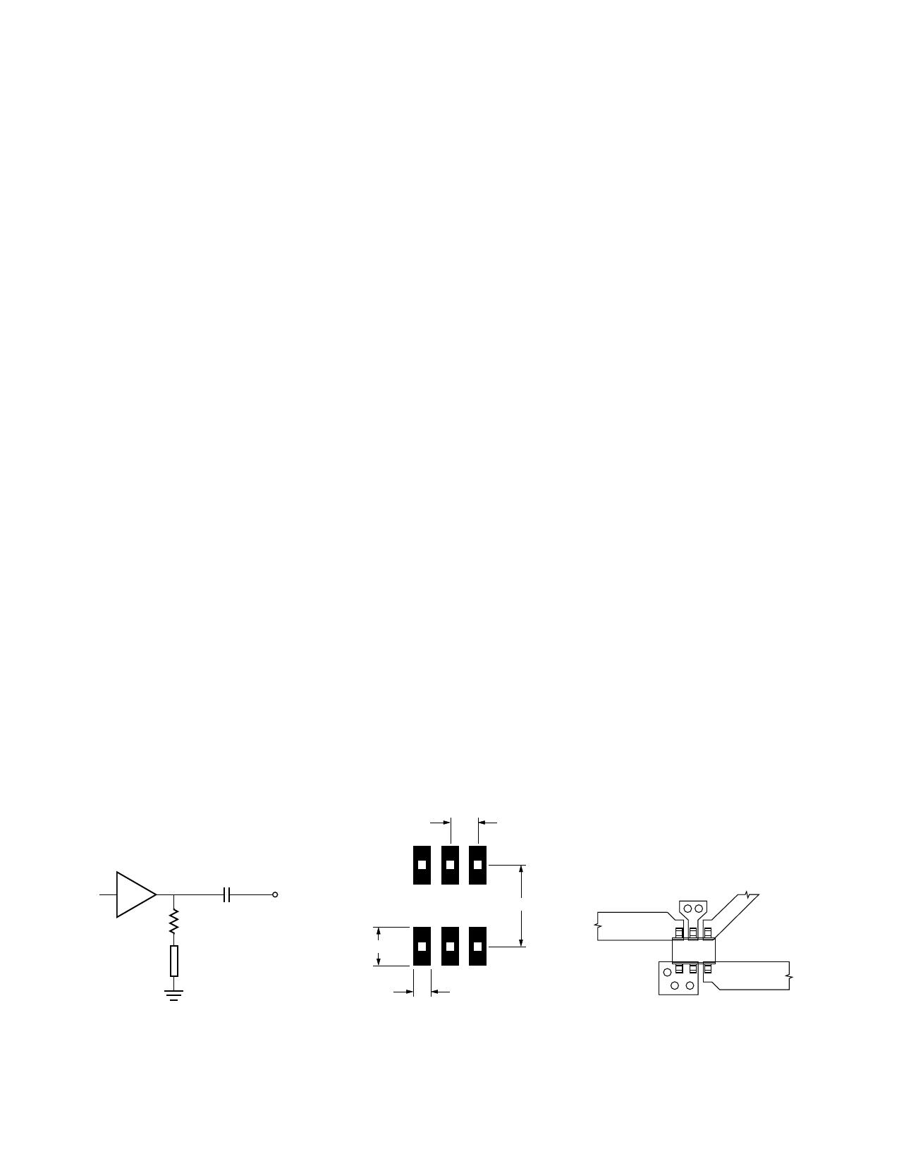
Stability
If the MGA-87563 is cascaded
with highly reactive stages (such
as filters) some precautions may
be needed to ensure stability. The
low frequency stability (under
1.5 GHz) of the MGA-87563 can
be enhanced by adding a series
R-L network in shunt with the
output, as shown in Figure 12.
The inductor can be either a chip
component or a high impedance
transmission line as shown in the
figure. Component values are
selected such that the output of
the MGA-87563 will be resistively
loaded at low frequencies while
allowing high frequency signals to
pass the stability load with
minimal loss.
Typical values for the resistor are
in the 25 to 50 Ω range. A
suggested starting place for the
inductor is a 0.35 to 0.40-inch long
microstripline with a width of
0.020 inches, using 0.031-inch
thick FR-4 (εr = 4.8) circuit board
as the substrate.
For applications near 1.5 GHz,
gain (and output power) may be
traded off for increased stability.
Some precautions regarding the
Vdd connection of the MGA-87563
are also recommended to ensure
stability within the operating
frequency range of the device. It
is important that the connection
to the power supply be properly
bypassed to realize full amplifier
performance. Refer to the Biasing
section above for more
information.
SOT-363 PCB Layout
A PCB pad layout for the minia-
ture SOT-363 (SC-70) package is
shown in Figure 13 (dimensions
are in inches). This layout provides
ample allowance for package
placement by automated assem-
bly equipment without adding
parasitics that could impair the
high frequency RF performance
of the MGA-87563. The layout is
shown with a nominal SOT-363
package footprint superimposed
on the PCB pads.
RF Layout
The RF layout in Figure 14 is
suggested as a starting point for
designs using the MGA-87563
amplifier. Adequate grounding is
needed to obtain maximum per-
formance and to obviate potential
instability. All three ground pins
of the MMIC should be connected
to RF ground by using plated
through holes (vias) near the
package terminals.
It is recommended that the PCB
traces for the ground pins NOT be
connected together underneath
the body of the package. PCB
pads hidden under the package
cannot be adequately inspected
for SMT solder quality.
FR-4 or G-10 PCB material is a
good choice for most low cost
wireless applications. Typical
board thickness is 0.025 or
0.031 inches. The width of 50 Ω
microstriplines in these PCB
thicknesses is also convenient for
mounting chip components such
as the series inductor at the input
0.026
MGA
87563
DC BLOCKING
CAPACITOR
25-50 Ω
RF
OUTPUT
HIGH IMPEDANCE
TRANSMISSION
OR INDUCTOR
Figure 12. Output Circuitry for Low
Frequency Stability.
0.07
0.035
0.016
Figure 13. PCB Pad Layout
(dimensions in inches).
RF OUTPUT
50 Ω
87
Figure 14. RF Layout.
VDD
50 Ω
RF INPUT
Share Link: 