NX25F011B Ver la hoja de datos (PDF) - Unspecified
Número de pieza
componentes Descripción
Fabricante
NX25F011B Datasheet PDF : 37 Pages
| |||
NX25F011B
NX25F021B
NX25F041B
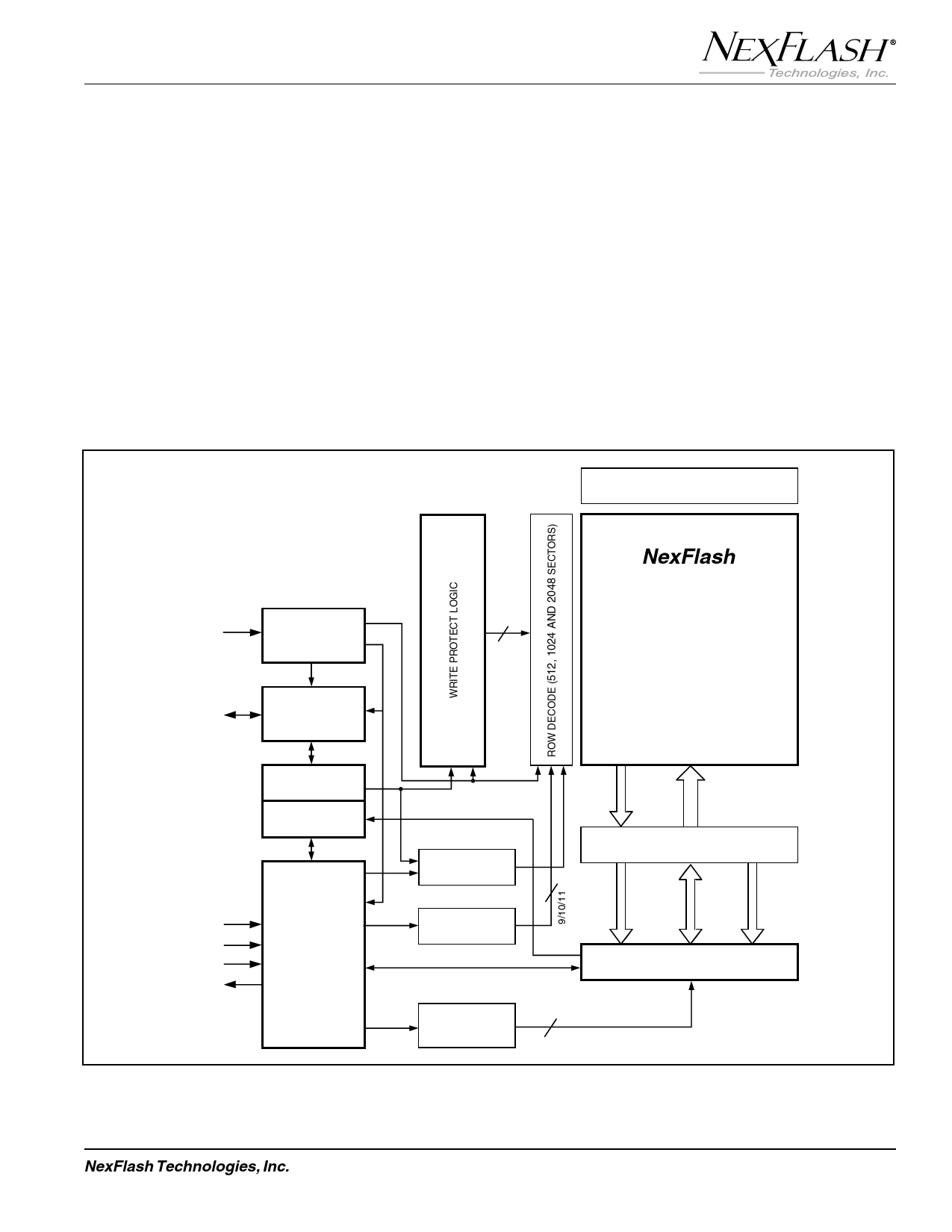
FUNCTIONAL OVERVIEW
An architectural block diagram of the NX25F011B,
NX25F021B, and NX25F041B is shown in Figure 2. Key
elements of the architecture include:
• SPI Interface and Command Set Logic
• Serial Flash Memory Array
• Serial SRAM and Program Buffer
• Write Protection Logic
• Configuration and Status Registers
• Device Information Sector
Pin Descriptions
1 Package
The NX25F011B, NX25F021B, and NX25F041B are
available in a 28-pin TSOP (Type I) surface mount package.
The NX25F011B and NX25F021B are available in either an
2 8-pin SOIC and a 14-pin TSOP package (contact NexFlash
for information on the 14-pin TSOP package). The
NX25F041B is also available in a 28-pin SOIC package.
See Figure 3A, 3B and Table 1 for pin assignments. All
interface and supply pins are on one side of the TSOP
3 package. The “No Connect” (NC) pins are not connected to
the device, allowing the pads and the area around them to
be used for routing PCB system traces. The devices are
also available in a cost-effective and space-efficient
removable Serial Flash Module package.
4
DEVICE INFORMATION SECTOR (DIS)
(READ ONLY)
WP
HOLD
OR R/B
WRITE CONTROL
LOGIC
HOLD OR
READ/BUSY
LOGIC
NexFlash
1, 2 AND 4 M-BIT
SERIAL FLASH MEMORY ARRAY
16
512, 1024 AND 2048
BYTE-ADDRESSABLE
SECTORS OF 264 BYTES EACH
ORGANIZED IN 16, 32, AND 64
BLOCKS OF 32 SECTORS PER BLOCK
CONFIGURATION
REGISTER
STATUS
REGISTER
HIGH-VOLTAGE
GENERATORS
2112
SRAM (264 BYTES)
SCK
CS
SI
SO
SPI
COMMAND
AND
CONTROL
LOGIC
SECTOR-ADDRESS
LATCH
DATA
BYTE-ADDRESS
LATCH/COUNTER
8
8
8
COLUMN DECODE, SENSE AMP LATCH
AND DATA COMPARE LOGIC
9
Figure 2. NX25F011B, NX25F021B, and NX25F041B Architectural Block Diagram
5
6
7
8
9
10
11
12
NexFlash Technologies, Inc.
5
PRELIMINARY NXSF016F-1201
12/12/01 ©
Share Link: 