MV8870 Ver la hoja de datos (PDF) - Zarlink Semiconductor Inc
Número de pieza
componentes Descripción
Fabricante
MV8870 Datasheet PDF : 12 Pages
| |||
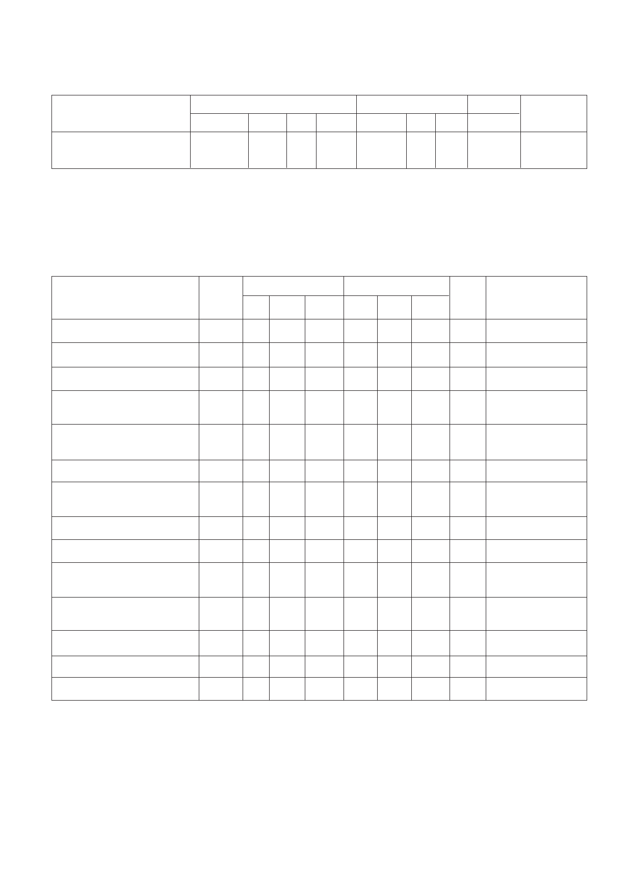
RECOMMENDED OPERATING RANGE
Characteristic
Positive supply voltage
Operating temperature
Value (MV8870)
Symbol
Min Typ Max
VDD
4.75 5.0 5.25
TOP
-40 +25 +80
MV8870/MV8870-1
Value (MV8870-1)
Min Typ Max Units
4.75 5.0 5.25 V
-40 +25 +80 ˚C
Conditions
ELECTRICAL CHARACTERISTICS Over Recommended Operating Range (unless otherwise specified)
These characteristics are guaranteed over the following conditions (unless otherwise stated):
Voltages measured with respect to ground (VSS).
Typical figures are for design aid only; they are not guaranteed and are not subject to production testing.
STATIC CHARACTERISTICS
Characterlstlc
Value (MV8870)
Symbol
Min Typ Max
Value (MV8870-1)
Mln Typ Max
Unlts
Conditions
Power dissipation
PD
VDD supply current
IDD
Input high voltage (OSC1 &
VIH
Input low voltage (OSC1 and VIL
TOE)
15
3.0
3.5
0
35
15
7.0
3.0
VDD
3.5
1.5 0
37 mW f0 = 3.579545MHZ
7.0 mA
VDD
V
1.5 V
Input leakage current (OSC1, ll
100
IN + and IN-)
100
mA
0 ≤ VPIN ≤ VDD
Internal pull-up current (TOE) IPU
Steering threshold voltage
VTSt
(St/GT)
7.5
15.0
7.5
15.0 µA
2.2 2.35 2.5 2.2 2.35 2.5 V
0 ≤ VPIN ≤ VDD
Low level output voltage
VOL
High level output voltage
VOH
Output low sink current (OSC2, IOL
Q1-Q4, StD and ESt)
0.03
4.97
1.0 2.5
0.03
4.97
1.0 2.5
V
No Load
V
No Load
mA
VPIN = 0.4V
Output high source current
IOH
(OSC2, Q1-Q4, StD and ESt)
0.4 0.8
0.4 0.8
mA
VPIN = 4.6V
Reference voltage
VREF output resistance
Pin capacitance
VREF
2.4
2.7 2.4
RREF
10.0
10.0
CP
7.0
15.0
7.0
2.8 V
kΩ
15.0 pF
No Load
Pin to supplies
7
Share Link: 