MCP6001T-E/SL Ver la hoja de datos (PDF) - Microchip Technology
Número de pieza
componentes Descripción
Fabricante
MCP6001T-E/SL Datasheet PDF : 28 Pages
| |||
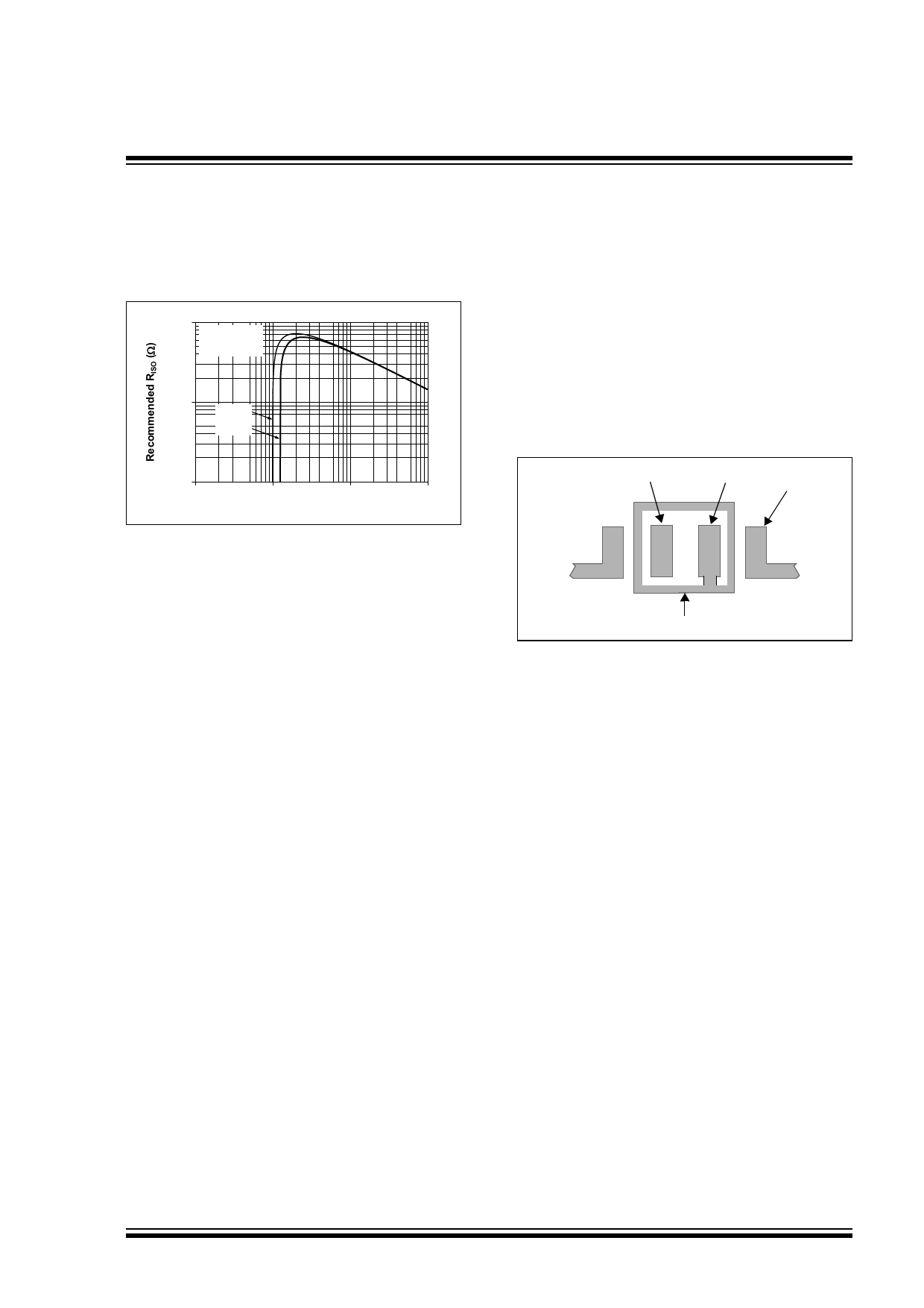
Figure 4-4 gives recommended RISO values for
different capacitive loads and gains. The x-axis is the
normalized load capacitance (CL/GN), where GN is the
circuit's noise gain. For non-inverting gains, GN and the
Signal Gain are equal. For inverting gains, GN is
1+|Signal Gain| (e.g., -1 V/V gives GN = +2 V/V).
1000
VDD = 5.0V
RL = 100 k:
100
GN = 1
GN t 2
10
11.E0-p11
11.E00-1p0
1.E1n-09
111.E00-nn08
Normalized Load Capacitance; CL/GN (F)
FIGURE 4-4:
Recommended RISO values
for Capacitive Loads.
After selecting RISO for your circuit, double-check the
resulting frequency response peaking and step
response overshoot. Modify RISO’s value until the
response is reasonable. Bench evaluation and simula-
tions with the MCP6001/2/4 SPICE macro model are
very helpful.
4.4 Supply Bypass
With this family of operational amplifiers, the power
supply pin (VDD for single-supply) should have a local
bypass capacitor (i.e., 0.01 µF to 0.1 µF) within 2 mm
for good high-frequency performance. It also needs a
bulk capacitor (i.e., 1 µF or larger) within 100 mm to
provide large, slow currents. This bulk capacitor can be
shared with other analog parts.
MCP6001/2/4
4.5 PCB Surface Leakage
In applications where low input bias current is critical,
Printed Circuit Board (PCB) surface leakage effects
need to be considered. Surface leakage is caused by
humidity, dust or other contamination on the board.
Under low humidity conditions, a typical resistance
between nearby traces is 1012Ω. A 5V difference would
cause 5 pA of current to flow; which is greater than the
MCP6001/2/4 family’s bias current at 25°C (1 pA, typ.).
The easiest way to reduce surface leakage is to use a
guard ring around sensitive pins (or traces). The guard
ring is biased at the same voltage as the sensitive pin.
An example of this type of layout is shown in
Figure 4-5.
VIN-
VIN+
VSS
Guard Ring
FIGURE 4-5:
Example Guard Ring Layout
for Inverting Gain.
1. Non-inverting Gain and Unity-Gain Buffer:
a. Connect the non-inverting pin (VIN+) to the
input with a wire that does not touch the
PCB surface.
b. Connect the guard ring to the inverting input
pin (VIN–). This biases the guard ring to the
common mode input voltage.
2. Inverting Gain and Transimpedance Gain
Amplifiers (convert current to voltage, such as
photo detectors):
a. Connect the guard ring to the non-inverting
input pin (VIN+). This biases the guard ring
to the same reference voltage as the op
amp (e.g., VDD/2 or ground).
b. Connect the inverting pin (VIN–) to the input
with a wire that does not touch the PCB
surface.
© 2005 Microchip Technology Inc.
DS21733F-page 9
Share Link: 