MAX9205(2001) Ver la hoja de datos (PDF) - Maxim Integrated
Número de pieza
componentes Descripción
Fabricante
MAX9205 Datasheet PDF : 13 Pages
| |||
10-Bit Bus LVDS Serializers
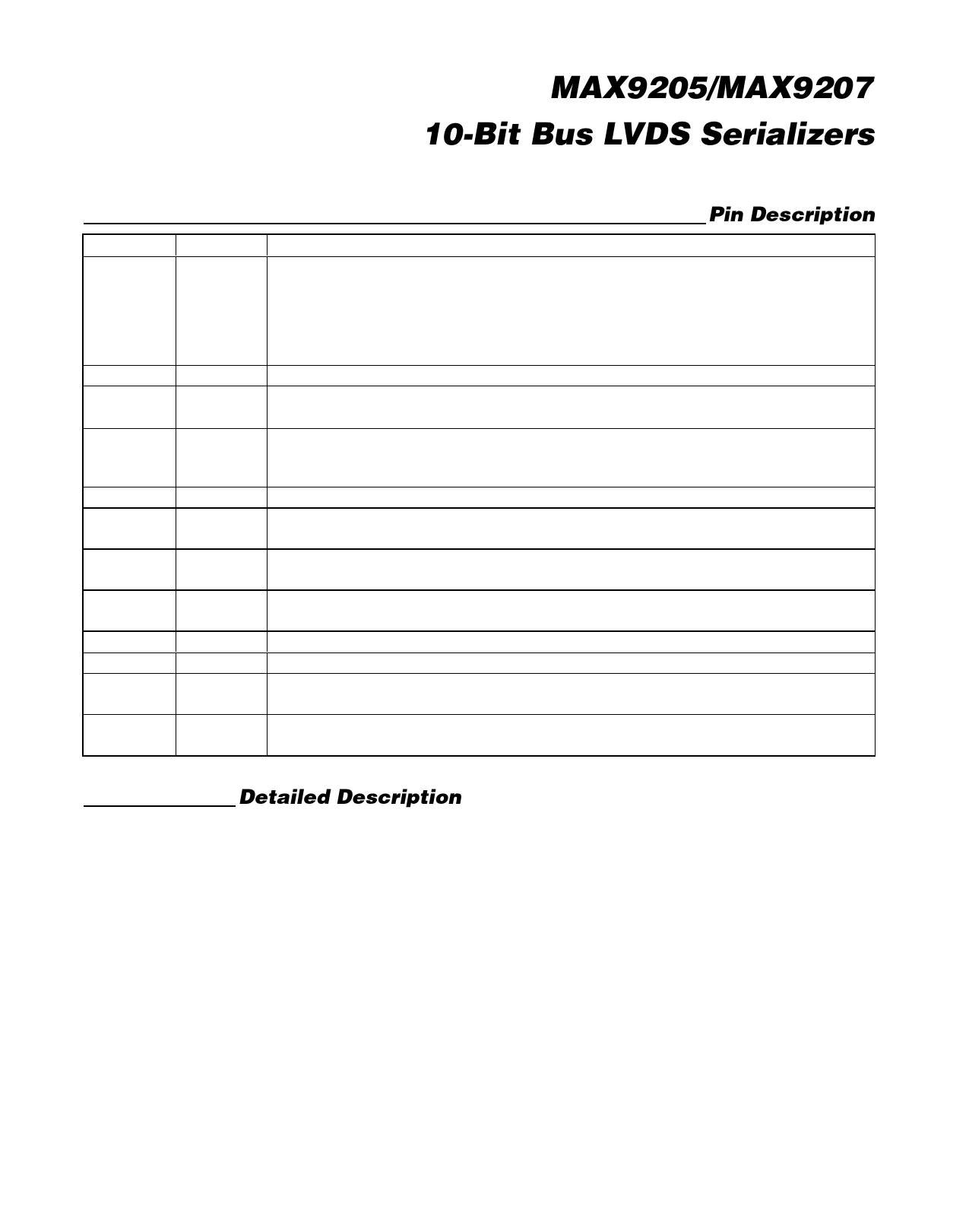
PIN
1, 2
3–12
13
14
15, 16
17, 26
18, 20,
23, 25
19
21
22
24
27, 28
Pin Description
NAME
SYNC 1,
SYNC 2
IN0–IN9
TCLK_R/F
TCLK
DGND
AVCC
AGND
FUNCTION
LVCMOS/LVTTL Logic Inputs. The two SYNC pins are ORed. When at least one of the two pins
are asserted high for at least six cycles of TCLK, the serializer initiates a transmission of 1024
SYNC patterns. If held high after 1024 SYNC patterns have been transmitted, SYNC patterns
continue to be sent until the SYNC pin is asserted low. Toggling a SYNC pin after six TCLK cycles
high and before 1024 SYNC patterns have been transmitted does not affect the output of the 1024
SYNC patterns.
LVCMOS/LVTTL Data Inputs. Data is loaded into a 10-bit latch by the selected TCLK edge.
LVCMOS/LVTTL Logic Input. High selects a TCLK rising-edge data strobe. Low selects a TCLK
falling-edge data strobe.
LVCMOS/LVTTL Reference Clock Input. The MAX9205 accepts a 16MHz to 40MHz clock. The
MAX9207 accepts a 40MHz to 66MHz clock. TCLK provides a frequency reference to the PLL and
strobes parallel data into the input latch.
Digital Circuit Ground. Connect to ground plane.
Analog Circuit Power Supply (Includes PLL). Bypass AVCC to ground with a 0.1µF capacitor and a
0.001µF capacitor. Place the 0.001µF capacitor closest to AVCC.
Analog Circuit Ground. Connect to ground plane.
EN
OUT-
OUT+
PWRDN
DVCC
LVCMOS/LVTTL Logic Input. High enables serial data output. Low puts the bus LVDS output into
high impedance.
Inverting Bus LVDS Differential Output
Noninverting Bus LVDS Differential Output
LVCMOS/LVTTL Logic Input. Low puts the device into power-down mode and the output into high
impedance.
Digital Circuit Power Supply. Bypass DVCC to ground with a 0.1µF capacitor and a 0.001µF
capacitor. Place the 0.001µF capacitor closest to DVCC.
Detailed Description
The MAX9205/MAX9207 are 10-bit serializers designed
to transmit data over balanced media that may be a
standard twisted-pair cable or PC board traces at
160Mbps to 660Mbps. The interface may be double-
terminated point-to-point or a heavily loaded multipoint
bus. The characteristic impedance of the media and
connected devices can range from 100Ω for a point-to-
point interface to 54Ω for a heavily loaded multipoint
bus. A double-terminated point-to-point interface uses
a 100Ω-termination resistor at each end of the inter-
face, resulting in a load of 50Ω. A heavily loaded multi-
point bus requires a termination as low as 54Ω at each
end of the bus, resulting in a termination load of 27Ω.
The serializer requires a deserializer such as the
MAX9206/MAX9208 for a complete data transmission
application.
A high-state start bit and a low-state stop bit, added
internally, frame the 10-bit parallel input data and
ensure a transition in the serial data stream. Therefore,
12 serial bits are transmitted for each 10-bit parallel
input. The MAX9205 accepts a 16MHz to 40MHz refer-
ence clock, producing a serial data rate of 192Mbps
(12 bits x 16MHz) to 480Mbps (12 bits x 40MHz). The
MAX9207 accepts a 40MHz to 66MHz reference clock,
producing 480Mbps to 792Mbps. However, since only
10 bits are from input data, the actual throughput is 10
times the TCLK frequency.
To transmit data, the serializers sequence through
three modes: initialization mode, synchronization mode,
and data transmission mode.
_______________________________________________________________________________________ 5
Share Link: 