MAX8739(2006) Ver la hoja de datos (PDF) - Maxim Integrated
Número de pieza
componentes Descripción
Fabricante
MAX8739 Datasheet PDF : 19 Pages
| |||
TFT, LCD, DC-DC Converter with
Operational Amplifiers
ABSOLUTE MAXIMUM RATINGS
IN, CTL, FREQ, LDO to AGND .................................-0.3V to +6V
COMP, FB, DEL to AGND ........................-0.3V to (VLDO + 0.3V)
PGND to AGND ..................................................................±0.3V
LX to PGND ............................................................-0.3V to +14V
SUP to AGND .........................................................-0.3V to +14V
POS1, POS2, NEG1, NEG2, OUT1,
OUT2 to AGND .....................................-0.3V to (VSUP + 0.3V)
SRC to AGND .........................................................-0.3V to +30V
COM, DRN to AGND ................................-0.3V to (VSRC + 0.3V)
COM RMS Output Current................................................±50mA
OUT1, OUT2 Maximum Continuous Output Current ........±75mA
LX Switch Maximum Continuous RMS Output Current .........1.6A
Continuous Power Dissipation (TA = +70°C)
20-Pin, 5mm × 5mm, Thin QFN (derate 20.8mW/°C
above +70°C).............................................................1667mW
Operating Temperature Range ...........................-40°C to +85°C
Junction Temperature ......................................................+150°C
Storage Temperature Range .............................-65°C to +150°C
Lead Temperature (soldering, 10s) .................................+300°C
Stresses beyond those listed under “Absolute Maximum Ratings” may cause permanent damage to the device. These are stress ratings only, and functional
operation of the device at these or any other conditions beyond those indicated in the operational sections of the specifications is not implied. Exposure to
absolute maximum rating conditions for extended periods may affect device reliability.
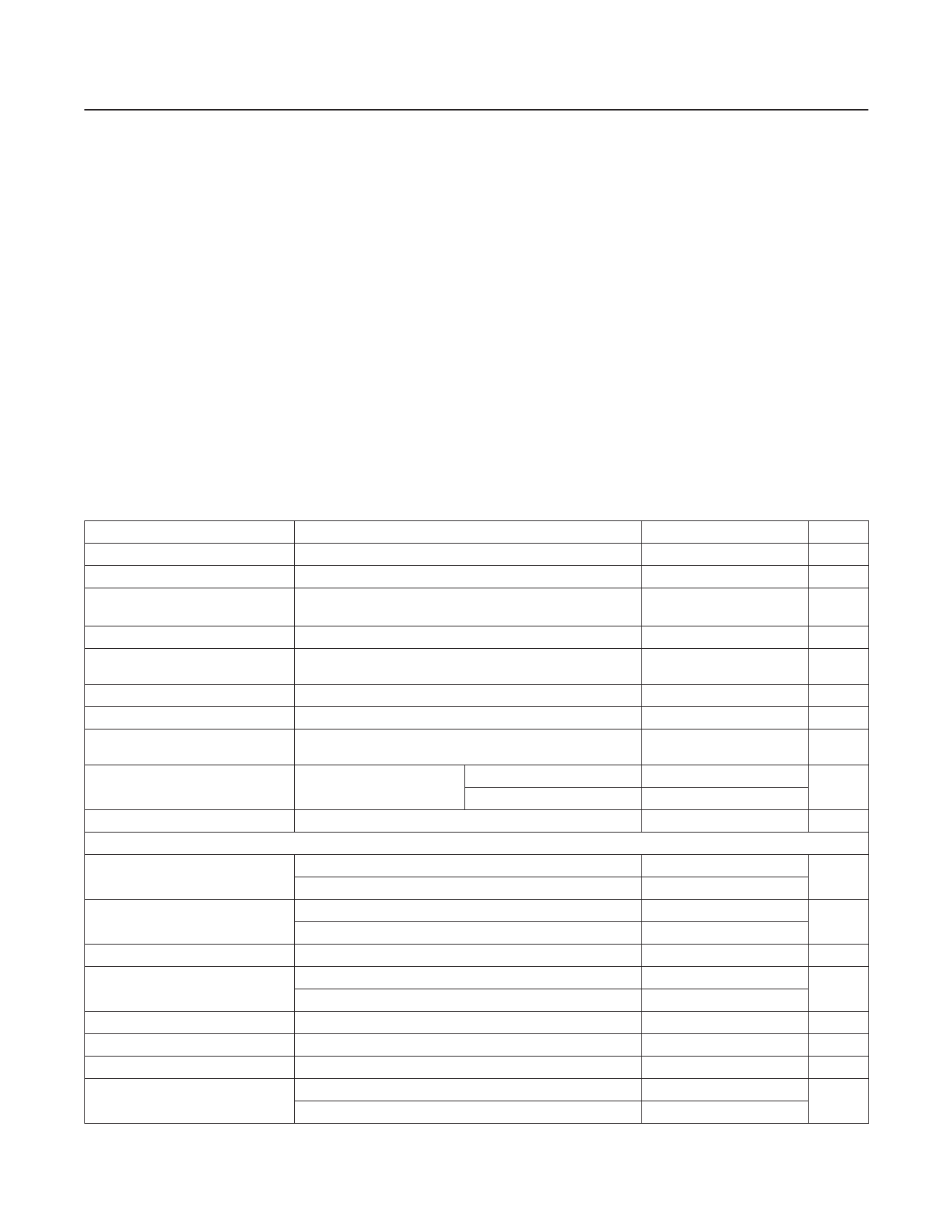
ELECTRICAL CHARACTERISTICS
(VIN = 2.5V, VSUP = 10V, VSRC = 28V, FREQ = CTL = IN, PGND = AGND = 0, TA = 0°C to +85°C. Typical values are at TA = +25°C,
unless otherwise noted.)
PARAMETER
IN Supply Range
IN Quiescent Current
IN Undervoltage Lockout
Threshold
LDO Output Voltage
LDO Undervoltage Lockout
Threshold
LDO Output Current
SUP Supply Voltage Range
SUP Undervoltage Fault
Threshold
SUP Supply Current
Thermal Shutdown
STEP-UP REGULATOR
Operating Frequency
Maximum Duty Cycle
FREQ Input Low Voltage
FREQ Input High Voltage
FREQ Pulldown Current
FB Regulation Voltage
FB Fault Trip Level
Duration to Trigger Fault
Condition
CONDITIONS
VIN = 2.5V, VFB = 1.5V
IN rising, 200mV hysteresis
6V ≤ VSUP ≤ 13V, ILDO = 12.5mA
LDO rising, 200mV hysteresis
VPOS_ = 4V, no load
LX not switching
LX switching
Rising edge, 15°C hysteresis
FREQ = AGND
FREQ = IN
FREQ = AGND
FREQ = IN
VIN = 1.8V to 5.5V
VIN = 1.8V to 2.4V
VIN = 2.4V to 5.5V
VFREQ = 1.0V
ISWITCH = 200mA
Falling edge
FREQ = AGND
FREQ = IN
MIN TYP MAX UNITS
1.8
5.5
V
15
30
µA
1.30 1.75
V
4.6
5
5.4
V
2.4
2.7
3.0
V
15
mA
4.5
13.0
V
1.4
V
1.8
3.0
mA
16
30
+160
°C
512
600
768
kHz
1020 1200 1380
91
95
99
%
88
92
96
0.6
V
1.4
V
2.0
3.5
5.0
6.0
µA
1.225 1.240 1.255
V
0.96 1.00 1.04
V
43
51
64
ms
47
55
65
2 _______________________________________________________________________________________
Share Link: 