MAX8862 Ver la hoja de datos (PDF) - Maxim Integrated
Número de pieza
componentes Descripción
Fabricante
MAX8862 Datasheet PDF : 12 Pages
| |||
Low-Cost, Low-Dropout, Dual Linear Regulator
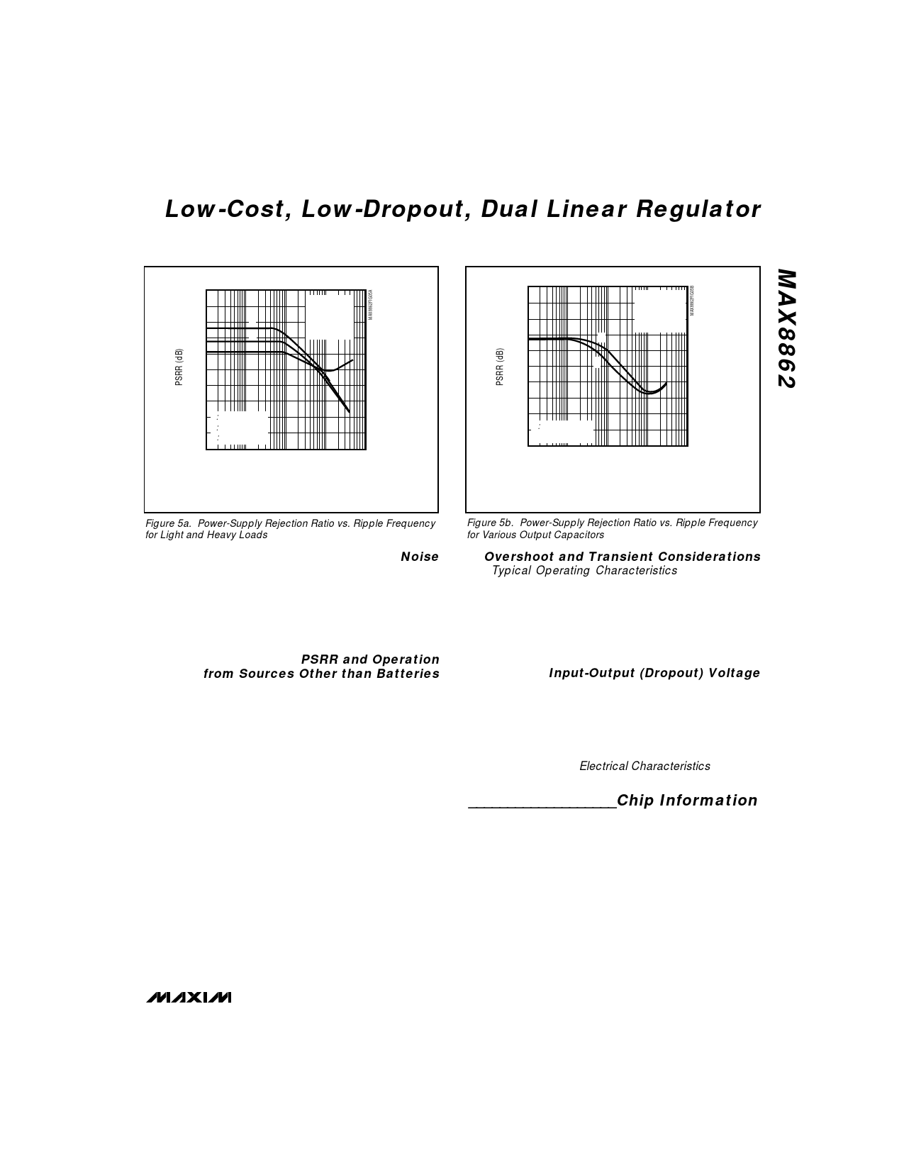
70
60
A
B
C
50
OUT1
∆VIN1 = 1Vp-p
CIN1 = 1µF
COUT1 = 3.3µF
40
30 A: IOUT1 = 1mA
B: IOUT1 = 10mA
C: IOUT1 = 100mA
20
0.01
0.1
1
10
100
FREQUENCY (kHz)
70
OUT1
65
∆VIN1 = 1Vp-p
60
CIN1 = 1µF
IOUT1 = 100mA
55
A
50
45
B
40
35
30
25 A: COUT1 = 100µF
B: COUT1 = 10µF
20
0.1
1
10
100
FREQUENCY (kHz)
1000
Figure 5a. Power-Supply Rejection Ratio vs. Ripple Frequency
for Light and Heavy Loads
Noise
The MAX8862’s OUT1 exhibits about 2.5mVp-p, and
OUT2 exhibits 1mVp-p of noise under full-load condi-
tions. When using the MAX8862 for applications that
include analog-to-digital converters (ADCs) with resolu-
tions greater than 12 bits, consider the ADC’s power-
supply-rejection specifications.
PSRR and Operation
from Sources Other than Batteries
The MAX8862 is designed to achieve low dropout volt-
ages and low quiescent currents in battery-powered
systems. However, to gain these benefits; the device
must trade away power-supply noise rejection, as well
as swift response to supply variations and load tran-
sients. For a 1mA load current, power-supply rejection
typically changes from 58dB to 43dB when the input
frequency is changed from 1Hz to 10kHz. At higher fre-
quencies, the circuit depends primarily on the output
capacitor’s characteristics, and the PSRR increases
(Figure 5).
When operating from sources other than batteries, sup-
ply-noise rejection and transient response can be
improved by increasing the value of the input and out-
put capacitors and employing passive filtering tech-
niques. Do not use power supplies with ripple voltages
exceeding 200mV at 100kHz.
Figure 5b. Power-Supply Rejection Ratio vs. Ripple Frequency
for Various Output Capacitors
Overshoot and Transient Considerations
The Typical Operating Characteristics section shows
power-up, line, and load-transient response graphs.
Typical transients for step changes in the load current
from 0mA to 300mA are 100mVp-p. During recovery
from shutdown, overshoot is minimized by the 1µF
input, and output capacitors (3.3µF for OUT1, and
2.2µF for OUT2).
Input-Output (Dropout) Voltage
A regulator’s minimum input-to-output voltage differen-
tial (or dropout voltage) determines the lowest usable
supply voltage. In battery-powered systems, this deter-
mines the useful end-of-life battery voltage. Since
P-channel MOSFETs are used as pass transistors, the
dropout voltage is the product of the RDS(ON) and the
load current (see the Electrical Characteristics).
___________________Chip Information
TRANSISTOR COUNT: 457
______________________________________________________________________________________ 11
Share Link: 