MAX864 Ver la hoja de datos (PDF) - Maxim Integrated
Número de pieza
componentes Descripción
Fabricante
MAX864 Datasheet PDF : 12 Pages
| |||
Dual-Output Charge Pump with Shutdown
_______________Detailed Description
The MAX864 requires only four external capacitors to
implement a voltage doubler/inverter. These may be
ceramic or polarized capacitors (electrolytic or tanta-
lum) with values ranging from 0.47µF to 100µF.
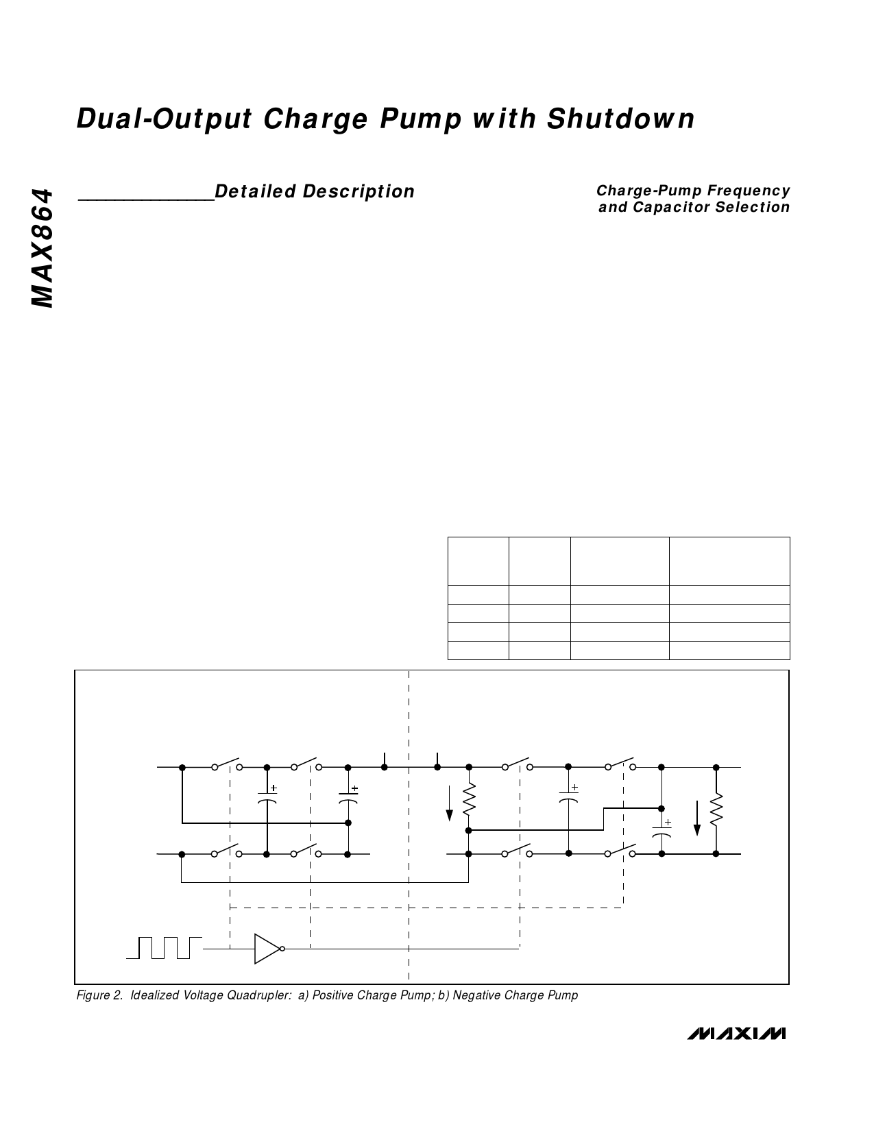
Figure 2a illustrates the ideal operation of the positive
voltage doubler. The on-chip oscillator generates a
50% duty-cycle clock signal. During the first half cycle,
switches S2 and S4 open, switches S1 and S3 close,
and capacitor C1 charges to the input voltage (VIN).
During the second half cycle, switches S1 and S3
open, switches S2 and S4 close, and capacitor C1 is
level shifted upward by VIN volts. Assuming ideal
switches and no load on C3, charge transfers into C3
from C1 such that the voltage on C3 will be 2VIN , gen-
erating the positive supply output (V+).
Figure 2b illustrates the ideal operation of the negative
converter. The switches of the negative converter are
out of phase from the positive converter. During the
second half cycle, switches S6 and S8 open, and
switches S5 and S7 close, charging C2 from V+
(pumped up to 2VIN by the positive charge pump) to
GND. In the first half of the clock cycle, switches S5
and S7 open, switches S6 and S8 close, and the
charge on capacitor C2 transfers to C4, generating the
negative supply. The eight switches are CMOS power
MOSFETs. Switches S1, S2, S4, and S5 are P-channel
devices, while switches S3, S6, S7, and S8 are N-chan-
nel devices.
Charge-Pump Frequency
and Capacitor Selection
The MAX864 offers four different charge-pump frequen-
cies. To select a desired frequency, define pins FC0 and
FC1 as shown in Table 1. Lower charge-pump frequen-
cies produce lower average supply currents, while high-
er charge-pump frequencies require smaller capacitors.
Table 1 also lists the recommended charge-pump
capacitor values for each pump frequency. Using val-
ues larger than those recommended will have little
effect on the output current. Using values smaller than
those recommended will reduce the available output
current and increase the output ripple. To cut the out-
put ripple in half, double the values of C3 and C4.
To maintain the lowest output resistance, use capacitors
with low effective series resistance (ESR). At each switch-
ing frequency, the charge-pump output resistance is a
function of C1, C2, C3, and C4’s ESR. Minimizing the
charge-pump capacitors’ ESR minimizes output resis-
tance. Use ceramic capacitors for best results.
Table 1. Frequency Selection
FC1
FC0
FREQUENCY
(kHz)
CAPACITORS
C1–C4
(µF)
0
0
7
33
0
1
33
6.8
1
0
100
2.2
1
1
185
1
a)
IN
GND
S1
C1+ S2
C1
C3
S3
S4
C1-
b)
V+
V+
S5
IL+
RL+
S7
IN
GND
C2+
S6
C2
IL-
C4
S8
C2-
GND
RL-
V-
Figure 2. Idealized Voltage Quadrupler: a) Positive Charge Pump; b) Negative Charge Pump
6 _______________________________________________________________________________________
Share Link: 