MAX864 Ver la hoja de datos (PDF) - Maxim Integrated
Número de pieza
componentes Descripción
Fabricante
MAX864 Datasheet PDF : 12 Pages
| |||
Dual-Output Charge Pump with Shutdown
____________________________Typical Operating Characteristics (continued)
(VIN = 5.0V, capacitor values in Table 1, TA = +25°C, unless otherwise noted.)
TIME TO EXIT SHUTDOWN
+5V
0V
+10V
FC0 = FC1 = IN (185kHz), C1–C4 = 1µF
FC0 = FC1 = GND (7kHz), C1–C4 = 33µF
0V
-10V
1ms/div
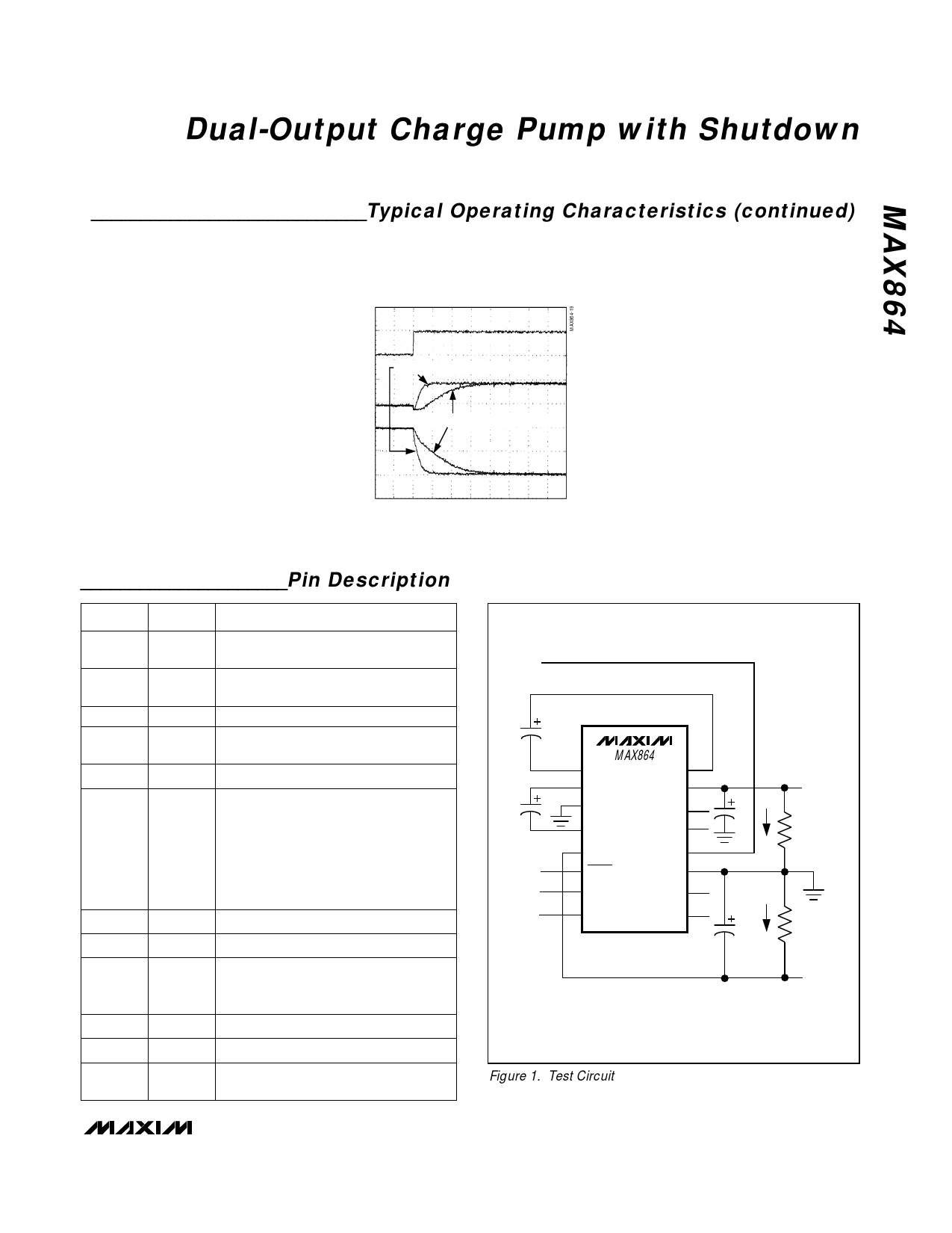
_____________________Pin Description
PIN
1
2
3, 11
4
5
6
7
8
9, 10,
13, 14
12
15
16
NAME
C1-
C2+
GND
C2-
V-
SHDN
FC1
FC0
N.C.
IN
V+
C1+
FUNCTION
Negative Terminal of the Flying Boost
Capacitor
Positive Terminal of the Flying
Inverting Capacitor
Ground (connect pins 3 and 11 together)
Negative Terminal of the Flying
Inverting Capacitor
Output of the Inverting Charge Pump
Active-Low Shutdown Input. With
SHDN low, the part is in shutdown
mode and its supply current is less
than 1µA. In shutdown mode, V+
connects to IN through a 22Ω switch,
and V- connects to GND through a
6Ω switch.
Frequency Select, MSB (see Table 1)
Frequency Select, LSB (see Table 1)
No Connect—no internal connection.
Connect these to ground to improve
thermal dissipation.
Positive Power-Supply Input
Output of the Boost Charge Pump
Positive Terminal of the Flying Boost
Capacitor
VCC IN
C1
C2
+5V
MAX864
1 C1-
C1+ 16
2 C2+
3
GND
V+ 15
N.C. 14
4 C2-
N.C. 13
5 V-
6 SHDN
7 FC1
IN 12
GND 11
N.C. 10
8 FC0
N.C. 9
SEE TABLE 1 FOR CAPACITOR VALUES.
C3
IL+
V+ OUT
RL+
C4
RL-
IL-
V- OUT
Figure 1. Test Circuit
_______________________________________________________________________________________ 5
Share Link: 