MAX780A Ver la hoja de datos (PDF) - Maxim Integrated
Número de pieza
componentes Descripción
Fabricante
MAX780A Datasheet PDF : 12 Pages
| |||
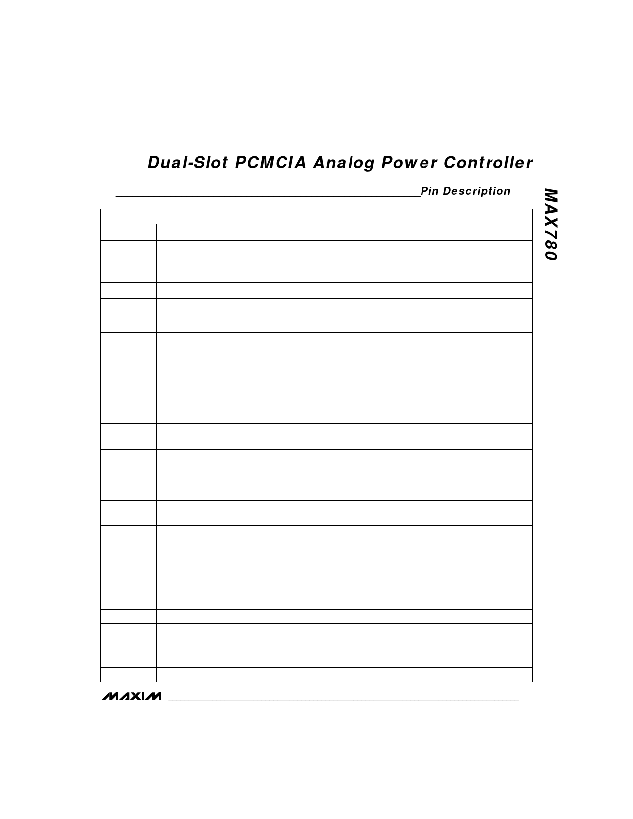
Dual-Slot PCMCIA Analog Power Controller
________________________________________________________Pin Description
PIN
MAX780A/B/C MAX780D
NAME
1
C2
2
3
4, 5
6, 7
8, 9
10, 11
12, 13
14, 15
16
17
1
C1
WR
2, 3
4, 5
6, 7
8, 9
10, 11
12, 13
AVPP1,
AVPP0
BVPP1,
BVPP0
AVCC1,
AVCC0
BVCC1,
BVCC0
BDRV5,
BDRV3
ADRV5,
ADRV3
BGPI
AGPI
18
14
SHDN
15
N.C.
19
REF
20
16
BVPP
21
17
AVPP
22
18
VCCIN
23
19
VPPIN
24
20
GND
FUNCTION
Pin-strap input that selects edge-triggered register or direct digital inputs. Tying C2 to
VCCIN makes the logic inputs edge triggered; inputs to pins 4-11 are clocked in on the
rising edge of WR. Tying C2 to GND allows control signals to be directly applied to the
logic inputs on pins 4-11. Connect to GND for MAX780C.
Pin-strap input that selects one of two logic decode modes for the digital inputs. See Tables 1-3.
Write pulse input. When C2 is tied to VCCIN, a rising edge on WR clocks in the VCC
and VPP enables. When C2 is tied to GND, inputs to WR have no effect. Connect to
GND for MAX780C.
Logic inputs that control the voltage on AVPP.
Logic inputs that control the voltage on BVPP.
Logic inputs that control the state of the MOSFET gate drivers ADRV3 and ADRV5.
Logic inputs that control the state of the MOSFET gate drivers BDRV3 and BDRV5.
Open-drain gate driver outputs that control the MOSFETs that switch the VCC pin of slot
B to 0V, 3.0V/3.3V, or 5V.
Open-drain gate driver outputs that control the MOSFETs that switch the VCC pin of slot
A to 0V, 3.0V/3.3V, or 5V.
Logic-level power-ready output that stays low as long as BVPP is greater than 11.05V
(MAX780A and MAX780C only). Make no connection to this pin for MAX780B.
Logic-level power-ready output that stays low as long as AVPP is greater than 11.05V
(MAX780A and MAX780C only). Make no connection to this pin for MAX780B.
Logic input that shuts the MAX780 down to a low supply-current state when brought
low. Asserting SHDN forces ADRV3, BDRV3, ADRV5, BDRV5, REF, AGPI, and BGPI
low. All VPP inputs and outputs are functional for either state of SHDN. Program AVPP
and BVPP to 0V for lowest power consumption.
No connect. Not internally connected.
1.25V reference voltage output (MAX780A and MAX780C only). Make no connection to
this pin for MAX780B.)
Switched output that provides 0V, 5V, or 12V to the VPP pins of slot B.
Switched output that provides 0V, 5V, or 12V to the VPP pins of slot A.
+5V power input
+12V power input. VPPIN can have 0V or 5V applied as long as VCCIN = 5V.
Ground
_______________________________________________________________________________________ 5
Share Link: 