M68AR024D Ver la hoja de datos (PDF) - STMicroelectronics
Número de pieza
componentes Descripción
Fabricante
M68AR024D Datasheet PDF : 19 Pages
| |||
M68AR024D
OPERATION
The M68AR024D has a Chip Enable power down
feature which invokes an automatic standby mode
whenever Chip Enable is de-asserted (E1 = High)
or Chip Select is asserted (E2 = Low), or UB/LB
are de-asserted (UB/LB = High). An Output En-
able (G) signal provides a high speed tri-state con-
trol, allowing fast read/write cycles to be achieved
with the common I/O data bus. Operational modes
are determined by device control inputs W, E1, LB
and UB as summarized in the Operating Modes ta-
ble (see Table 6).
Table 6. Operating Modes
Operation
E1 E2 W G LB UB DQ0-DQ7 DQ8-DQ15
Deselected/Standby
VIH X
X
X
X
X
Hi-Z
Hi-Z
Deselected/Standby
X VIL X
X
X
X
Hi-Z
Hi-Z
Deselected/Standby
X
X
X
X VIH VIH
Hi-Z
Hi-Z
Lower Byte Read
VIL VIH VIH VIL VIL VIH Data Output
Hi-Z
Lower Byte Write
VIL VIH VIL X VIL VIH Data Input
Hi-Z
Output Disabled
VIL VIH VIH VIH X
X
Hi-Z
Hi-Z
Upper Byte Read
VIL VIH VIH VIL VIH VIL
Hi-Z
Data Output
Upper Byte Write
VIL VIH VIL X VIH VIL
Hi-Z
Data Input
Word Read
VIL VIH VIH VIL VIL VIL Data Output Data Output
Word Write
VIL VIH VIL X VIL VIL Data Input Data Input
Note: 1. X = VIH or VIL.
Power
Standby (ISB)
Standby (ISB)
Standby (ISB)
Active (ICC)
Active (ICC)
Active (ICC)
Active (ICC)
Active (ICC)
Active (ICC)
Active (ICC)
Read Mode
The M68AR024D, when Chip Select (E2) is High,
is in the read mode whenever Write Enable (W) is
High with Output Enable (G) Low, and Chip En-
able (E1) is asserted. This provides access to data
from eight or sixteen, depending on the status of
the signal UB and LB, of the 16,777,216 locations
in the static memory array, specified by the 20 ad-
dress inputs. Valid data will be available at the
eight or sixteen output pins within tAVQV after the
last stable address, providing G is Low and E1 is
Low. If Chip Enable or Output Enable access
times are not met, data access will be measured
from the limiting parameter (tELQV, tGLQV or tBLQV)
rather than the address. Data out may be indeter-
minate at tELQX, tGLQX and tBLQX, but data lines
will always be valid at tAVQV
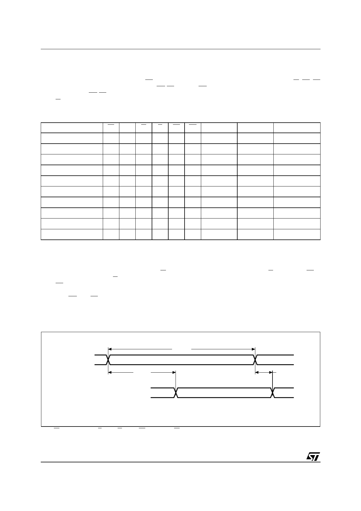
Figure 7. Address Controlled, Read Mode AC Waveforms
A0-A19
tAVQV
tAVAV
VALID
tAXQX
DQ0-DQ7 and/or DQ8-DQ15
DATA VALID
AI05403
Note: E1 = Low, E2 = High, G = Low, W = High, UB = Low and/or LB = Low.
8/19
Share Link: 