MAX7316 Ver la hoja de datos (PDF) - Maxim Integrated
Número de pieza
componentes Descripción
Fabricante
MAX7316
Maxim Integrated

MAX7316 Datasheet PDF : 24 Pages
| |||
10-Port I/O Expander with LED Intensity
Control, Interrupt, and Hot-Insertion Protection
The second (A5), third (A4), fourth (A3), sixth (A1), and
last (A0) bits of the MAX7316 slave address are always
1, 0, 0, 0, and 0. Slave address bits A6 and A2 are
selected by the address input AD0. AD0 can be con-
nected to GND, V+, SDA, or SCL. The MAX7316 has four
possible slave addresses (Table 1), and therefore a
maximum of four MAX7316 devices can be controlled
independently from the same interface.
Table 1. MAX7316 I2C Slave Address Map
DEVICE ADDRESS
PIN AD0
A6 A5 A4 A3 A2 A1 A0
SCL
1
1
0
0
0
0
0
SDA
1
1
0
0
1
0
0
GND
0
1
0
0
0
0
0
V+
0
1
0
0
1
0
0
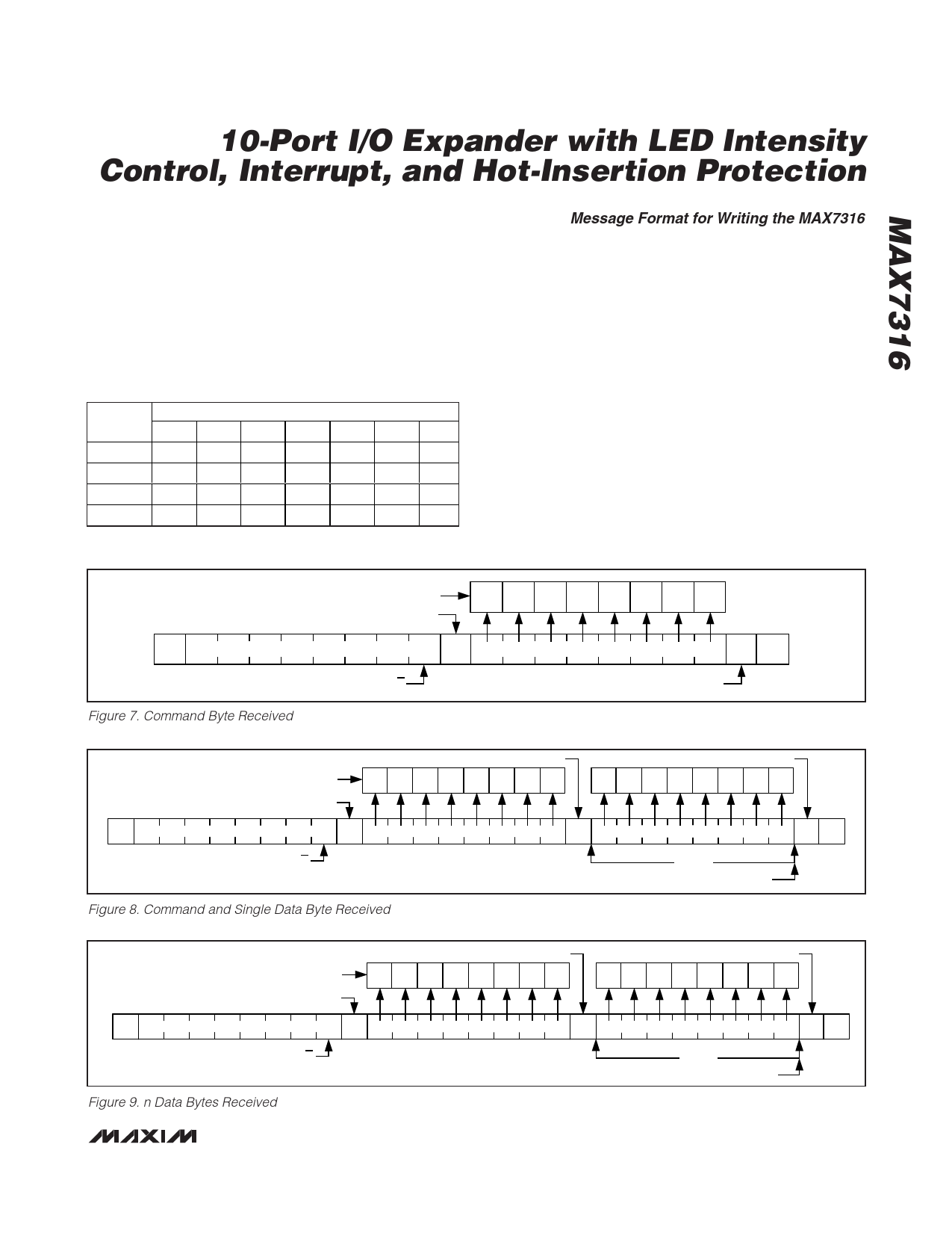
Message Format for Writing the MAX7316
A write to the MAX7316 comprises the transmission of
the MAX7316’s slave address with the R/W bit set to
zero, followed by at least 1 byte of information. The first
byte of information is the command byte. The com-
mand byte determines which register of the MAX7316
is to be written to by the next byte, if received (Table 2).
If a STOP condition is detected after the command byte
is received, then the MAX7316 takes no further action
beyond storing the command byte.
Any bytes received after the command byte are data
bytes. The first data byte goes into the internal register
of the MAX7316 selected by the command byte (Figure
8). If multiple data bytes are transmitted before a STOP
condition is detected, these bytes are generally stored
in subsequent MAX7316 internal registers because the
command byte address autoincrements (Table 2). A
diagram of a write to the output ports registers (blink
phase 0 register or blink phase 1 register) is given in
Figure 10.
COMMAND BYTE IS STORED ON RECEIPT OF
STOP CONDITION
ACKNOWLEDGE FROM MAX7316
D15 D14 D13 D12 D11 D10 D9 D8
S
SLAVE ADDRESS
0A
COMMAND BYTE
AP
R/W
Figure 7. Command Byte Received
ACKNOWLEDGE FROM MAX7316
HOW COMMAND BYTE AND DATA BYTE MAP INTO
MAX7316'S REGISTERS
ACKNOWLEDGE FROM MAX7316
ACKNOWLEDGE FROM MAX7316
D15 D14 D13 D12 D11 D10 D9 D8
ACKNOWLEDGE FROM MAX7316
D7 D6 D5 D4 D3 D2 D1 D0
S
SLAVE ADDRESS
0A
COMMAND BYTE
A
DATA BYTE
AP
1
R/W
BYTE
AUTOINCREMENT MEMORY ADDRESS
Figure 8. Command and Single Data Byte Received
HOW COMMAND BYTE AND DATA BYTE MAP INTO
MAX7316'S REGISTERS
ACKNOWLEDGE FROM MAX7316
ACKNOWLEDGE FROM MAX7316
D15 D14 D13 D12 D11 D10 D9 D8
ACKNOWLEDGE FROM MAX7316
D7 D6 D5 D4 D3 D2 D1 D0
S
SLAVE ADDRESS
0A
R/W
Figure 9. n Data Bytes Received
COMMAND BYTE
A
DATA BYTE
AP
N
BYTES
AUTOINCREMENT MEMORY ADDRESS
_______________________________________________________________________________________ 9
Share Link: