MAX7319 Ver la hoja de datos (PDF) - Maxim Integrated
Número de pieza
componentes Descripción
Fabricante
MAX7319 Datasheet PDF : 15 Pages
| |||
MAX7319
I2C Port Expander with Eight Inputs
and Maskable Transition Detection
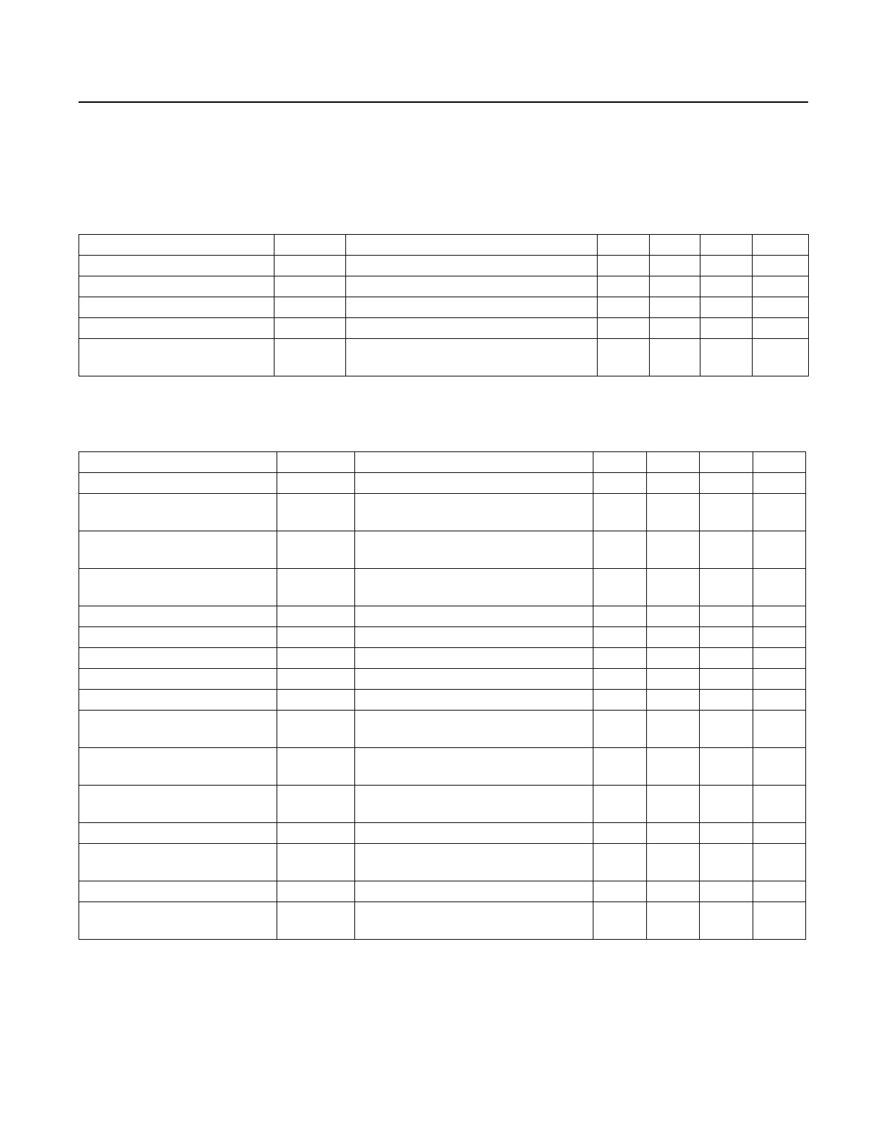
Port and Interrupt INT Timing Characteristics
(V+ = +1.71V to +5.5V, TA = -40°C to +125°C, unless otherwise noted. Typical values are at V+ = +3.3V, TA = +25°C.) (Note 1)
PARAMETER
SYMBOL
CONDITIONS
MIN TYP MAX UNITS
Port Input Setup Time
Port Input Hold Time
INT Input Data Valid Time
INT Reset Delay Time from STOP
INT Reset Delay Time from
Acknowledge
tPSU
tPH
tIV
tIP
tIR
CL ≤ 100pF
CL ≤ 100pF
CL ≤ 100pF
CL ≤ 100pF
CL ≤ 100pF
0
µs
4
µs
4
µs
4
µs
4
µs
Timing Characteristics
(V+ = +1.71V to +5.5V, TA = -40°C to +125°C, unless otherwise noted. Typical values are at V+ = +3.3V, TA = +25°C.) (Note 1)
PARAMETER
Serial-Clock Frequency
Bus Free Time Between a STOP
and a START Condition
Hold Time (Repeated) START
Condition
Repeated START Condition
Setup Time
STOP Condition Setup Time
Data Hold Time
Data Setup Time
SCL Clock Low Period
SCL Clock High Period
Rise Time of Both SDA and SCL
Signals, Receiving
Fall Time of Both SDA and SCL
Signals, Receiving
Fall Time of SDA, Transmitting
Pulse Width of Spike Suppressed
SYMBOL
fSCL
tBUF
CONDITIONS
tHD, STA
tSU, STA
tSU, STO
tHD, DAT
tSU, DAT
tLOW
tHIGH
(Note 2)
tR
(Notes 3, 4)
tF
(Notes 3, 4)
tF,TX
tSP
(Notes 3, 4)
(Note 5)
MIN TYP MAX UNITS
400
kHz
1.3
µs
0.6
µs
0.6
µs
0.6
µs
0.9
µs
100
ns
1.3
µs
0.7
µs
20 +
0.1Cb
300
ns
20 +
0.1Cb
300
ns
20 +
0.1Cb
250
ns
50
ns
Capacitive Load for Each Bus Line
Cb
(Note 3)
400
pF
RST Pulse Width
tW
500
ns
RST Rising to START Condition
Setup Time
tRST
1
µs
Note 1: All parameters are tested at TA = +25°C. Specifications over temperature are guaranteed by design.
Note 2: A master device must provide a hold time of at least 300ns for the SDA signal (referred to VIL of the SCL signal) to bridge
the undefined region of SCL’s falling edge.
Note 3: Guaranteed by design.
Note 4: Cb = total capacitance of one bus line in pF. tR and tF measured between 0.3 x V+ and 0.7 x V+, ISINK ≤ 6mA.
Note 5: Input filters on the SDA and SCL inputs suppress noise spikes less than 50ns.
www.maximintegrated.com
Maxim Integrated │ 3
Share Link: 