MAX7319 Ver la hoja de datos (PDF) - Maxim Integrated
Número de pieza
componentes Descripción
Fabricante
MAX7319 Datasheet PDF : 15 Pages
| |||
MAX7319
I2C Port Expander with Eight Inputs
and Maskable Transition Detection
Absolute Maximum Ratings
(All voltages referenced to GND.)
Supply Voltage V+....................................................-0.3V to +6V
SCL, SDA, AD0, AD2, RST, INT, I0–I7....................-0.3V to +6V
SDA Input Current.............................................................. 10mA
INT Input Current................................................................10mA
Total V+ Current..................................................................50mA
Total GND Current ............................................................100mA
Continuous Power Dissipation (TA = +70°C)
16-Pin QSOP (derate 8.3mW/°C over +70°C).............667mW
16-Pin TQFN (derate 15.6mW/°C over +70°C).........1250mW
Operating Temperature Range.......................... -40°C to +125°C
Junction Temperature.......................................................+150°C
Storage Temperature Range............................. -65°C to +150°C
Lead Temperature (soldering, 10s).................................. +300°C
Stresses beyond those listed under “Absolute Maximum Ratings” may cause permanent damage to the device. These are stress ratings only, and functional operation of the device at these
or any other conditions beyond those indicated in the operational sections of the specifications is not implied. Exposure to absolute maximum rating conditions for extended periods may affect
device reliability.
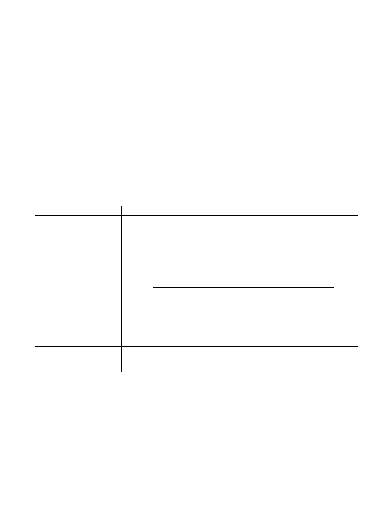
Electrical Characteristics
(V+ = +1.71V to +5.5V, TA = -40°C to +125°C, unless otherwise noted. Typical values are at V+ = +3.3V, TA = +25°C.) (Note 1)
PARAMETER
SYMBOL
CONDITIONS
MIN TYP MAX UNITS
Operating Supply Voltage
V+
1.71
5.50
V
Power-On Reset Voltage
Standby Current (Interface Idle)
Supply Current
(Interface Running)
VPOR
ISTB
I+
SCL and SDA and other digital inputs at V+
fSCL = 400kHz; other digital inputs at V+
1.6
V
0.6
1.5
µA
23
55
µA
Input High Voltage
SDA, SCL, AD0, AD2, RST, I0–I7
Input Low Voltage
SDA, SCL, AD0, AD2, RST, I0–I7
Input Leakage Current
SDA, SCL, AD0, AD2, RST, I0–I7
VIH
VIL
IIH, IIL
V+ < 1.8V
V+ ≥ 1.8V
V+ < 1.8V
V+ ≥ 1.8V
SDA, SCL, AD0, AD2, RST, I0–I7 at V+ or
GND
0.8 x V+
0.7 x V+
-0.2
V
0.2 x V+
V
0.3 x V+
+0.2
µA
Input Capacitance
SDA, SCL, AD0, AD2, RST, I0–I7
10
pF
Output Low Voltage
SDA
VOLSDA ISINK = 6mA
250
mV
Output Low Voltage
INT
VOLINT ISINK = 5mA
100 250
mV
Port Input Pullup Resistor
RPU
25
40
55
kW
www.maximintegrated.com
Maxim Integrated │ 2
Share Link: 