MAX7312 Ver la hoja de datos (PDF) - Maxim Integrated
Número de pieza
componentes Descripción
Fabricante
MAX7312
Maxim Integrated

MAX7312 Datasheet PDF : 16 Pages
| |||
2-Wire-Interfaced 16-Bit I/O Port Expander
with Interrupt and Hot-Insertion Protection
MAX7312 generates the acknowledge bit since the
MAX7312 is the recipient. When the MAX7312 is trans-
mitting to the master, the master generates the
acknowledge bit.
Slave Address
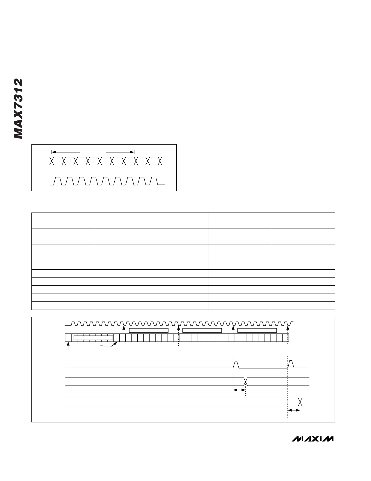
The MAX7312 has a 7-bit-long slave address (Figure 6).
The 8th bit following the 7-bit slave address is the R/W
bit. Set this bit low for a write command and high for a
read command.
SDA A6 A5
MSB
PROGRAMMABLE
A4 A3 A2
A1 A0 R/W ACK
LSB
SDA
Slave address pins AD2, AD1, and AD0 choose 1 of 64
slave ID addresses (Table 7).
Data Bus Transaction
The command byte is the first byte to follow the 8-bit
device slave address during a write transmission
(Table 1, Figure 7). The command byte is used to deter-
mine which of the following registers are written or read.
Writing to Port Registers
Transmit data to the MAX7312 by sending the device
slave address and setting the LSB to a logic zero. The
command byte is sent after the address and deter-
mines which registers receive the data following the
command byte (Figure 7).
Figure 6. Slave Address
Table 1. Command Byte Register
COMMAND BYTE
ADDRESS (HEX)
0x00
0x01
0x02
0x03
0x04
0x05
0x06
0x07
0x08
0xFF
FUNCTION
Input port 1
Input port 2
Output port 1
Output port 2
Port 1 polarity inversion
Port 2 polarity inversion
Port 1 configuration
Port 2 configuration
Timeout register
Factory reserved. (Do not write to this register.)
PROTOCOL
Read byte
Read byte
Read/write byte
Read/write byte
Read/write byte
Read/write byte
Read/write byte
Read/write byte
Read/write byte
—
POWER-UP
DEFAULT
XXXX XXXX
XXXX XXXX
1111 1111
1111 1111
0000 0000
0000 0000
1111 1111
1111 1111
0000 0001
—
SCL
123456789
COMMAND BYTE
PORT 1 DATA
PORT 2 DATA
SDA S
SLAVE ADDRESS
A 0 0 0 0 0 0 1 0A 7 6 5 4 3 2 1 0A 7 6 5 4 3 2 1 0 A
START
CONDITION
R/W
ACKNOWLEDGE
FROM SLAVE
ACKNOWLEDGE
FROM SLAVE
ACKNOWLEDGE
FROM SLAVE
ACKNOWLEDGE
FROM SLAVE
WRITE TO PORT
DATA OUT PORT 1
tPV
READ FROM PORT 2
tPV
Figure 7. Writes to Output Registers Through Write Byte Protocol
8 _______________________________________________________________________________________
Share Link: