MAX7312 Ver la hoja de datos (PDF) - Maxim Integrated
Número de pieza
componentes Descripción
Fabricante
MAX7312
Maxim Integrated

MAX7312 Datasheet PDF : 16 Pages
| |||
2-Wire-Interfaced 16-Bit I/O Port Expander
with Interrupt and Hot-Insertion Protection
SDA
SCL
S
START
CONDITION
Figure 3. START and STOP Conditions
P
STOP
CONDITION
SDA
SCL
Figure 4. Bit Transfer
START CONDITION
SCL
SDA
BY TRANSMITTER
DATA LINE STABLE; DATA VALID CHANGE OF DATA ALLOWED
1
2
CLOCK PULSE FOR ACKNOWLEDGMENT
8
9
S
SDA
BY RECEIVER
Figure 5. Acknowledge
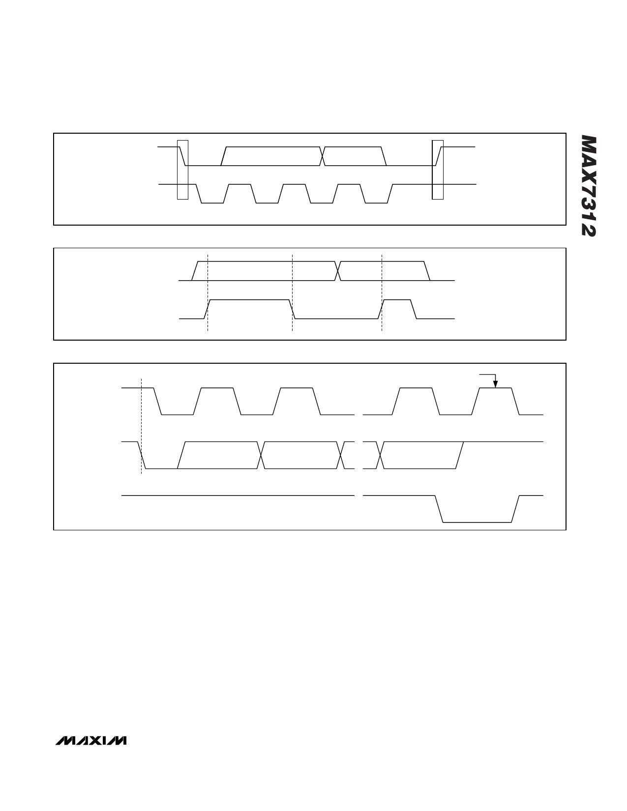
Each transmission consists of a START condition sent by
a master, followed by the MAX7312 7-bit slave address
plus R/W bit, a register address byte, 1 or more data
bytes, and finally a STOP condition (Figure 3).
START and STOP Conditions
Both SCL and SDA remain high when the interface is
not busy. A master signals the beginning of a transmis-
sion with a START (S) condition by transitioning SDA
from high to low while SCL is high. When the master
has finished communicating with the slave, it issues a
STOP (P) condition by transitioning SDA from low to
high while SCL is high. The bus is then free for another
transmission (Figure 3).
Bit Transfer
One data bit is transferred during each clock pulse.
The data on SDA must remain stable while SCL is high
(Figure 4).
Acknowledge
The acknowledge bit is a clocked 9th bit, which the
recipient uses as a handshake receipt of each byte of
data (Figure 5). Thus, each byte transferred effectively
requires 9 bits. The master generates the 9th clock
pulse, and the recipient pulls down SDA during the
acknowledge clock pulse, such that the SDA line is sta-
ble low during the high period of the clock pulse. When
the master is transmitting to the MAX7312, the
_______________________________________________________________________________________ 7
Share Link: