MAX7301(2003) Ver la hoja de datos (PDF) - Maxim Integrated
Número de pieza
componentes Descripción
Fabricante
MAX7301 Datasheet PDF : 18 Pages
| |||
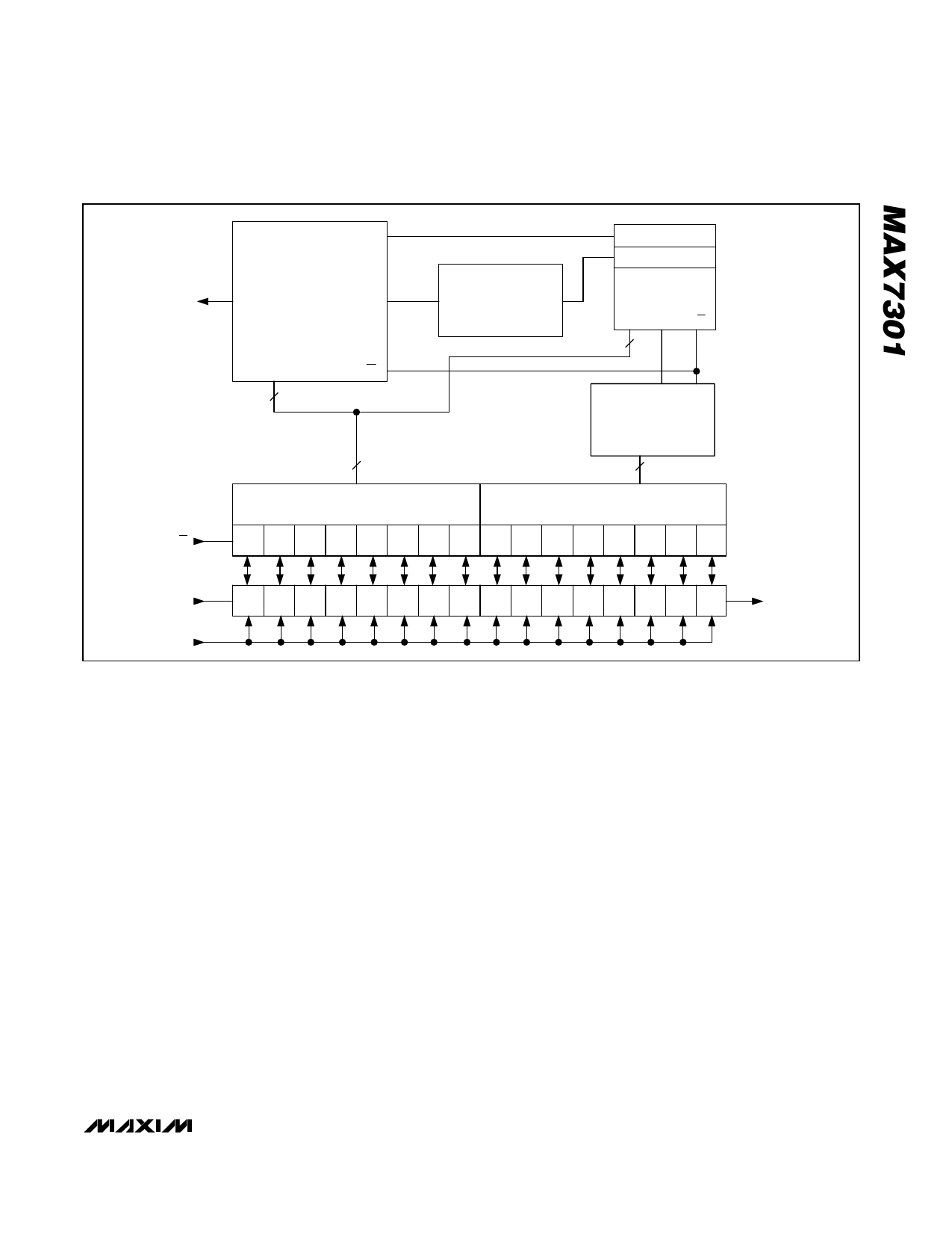
4-Wire-Interfaced, 2.5V to 5.5V, 20-Port and
28-Port I/O Expander
P4 TO P31
CS
CONFIGURATION
GPIO
GPIO DATA
R/W
8
PORT CHANGE
DETECTOR
PORT REGISTERS
MASK REGISTER
CONFIGURATION
REGISTERS
DATA CE R/W
8
COMMAND
REGISTER DECODE
8
8
DATA BYTE
COMMAND BYTE
D0 D1 D2 D3 D4 D5 D6 D7 D8 D9 D10 D11 D12 D13 D14 D15
DIN
D0 D1 D2 D3 D4 D5 D6 D7 D8 D9 D10 D11 D12 D13 D14 D15
DOUT
SCLK
Figure 1. MAX7301 Functional Diagram
The MAX7301 is written to using the following
sequence:
1) Take SCLK low.
2) Take CS low. This enables the internal 16-bit shift
register.
3) Clock 16 bits of data into DIN—D15 first, D0 last—
observing the setup and hold times (bit D15 is low,
indicating a write command).
4) Take CS high (either while SCLK is still high after
clocking in the last data bit, or after taking SCLK
low).
5) Take SCLK low (if not already low).
Figure 4 shows a write operation when 16 bits are
transmitted.
It is acceptable to clock more than 16 bits into the
MAX7301 between taking CS low and taking CS high
again. In this case, only the last 16 bits clocked into the
MAX7301 are retained.
Reading Device Registers
Any register data within the MAX7301 may be read by
sending a logic high to bit D15. The sequence is:
1) Take SCLK low.
2) Take CS low (this enables the internal 16-bit Shift
register).
3) Clock 16 bits of data into DIN—D15 first to D0 last.
D15 is high, indicating a read command and bits
D14 through D8 containing the address of the regis-
ter to be read. Bits D7–D0 contain dummy data,
which is discarded.
4) Take CS high (either while SCLK is still high after
clocking in the last data bit, or after taking SCLK
low), positions D7 through D0 in the Shift register
are now loaded with the register data addressed by
bits D1 through D8.
5) Take SCLK low (if not already low).
6) Issue another read or write command (which can
be a No-Op), and examine the bit stream at DOUT;
the second 8 bits are the contents of the register
addressed by bits D1 through D8 in step 3.
_______________________________________________________________________________________ 7
Share Link: 