MAX7033 Ver la hoja de datos (PDF) - Maxim Integrated
Número de pieza
componentes Descripción
Fabricante
MAX7033 Datasheet PDF : 16 Pages
| |||
MAX7033
315MHz/433MHz ASK Superheterodyne
Receiver with AGC Lock
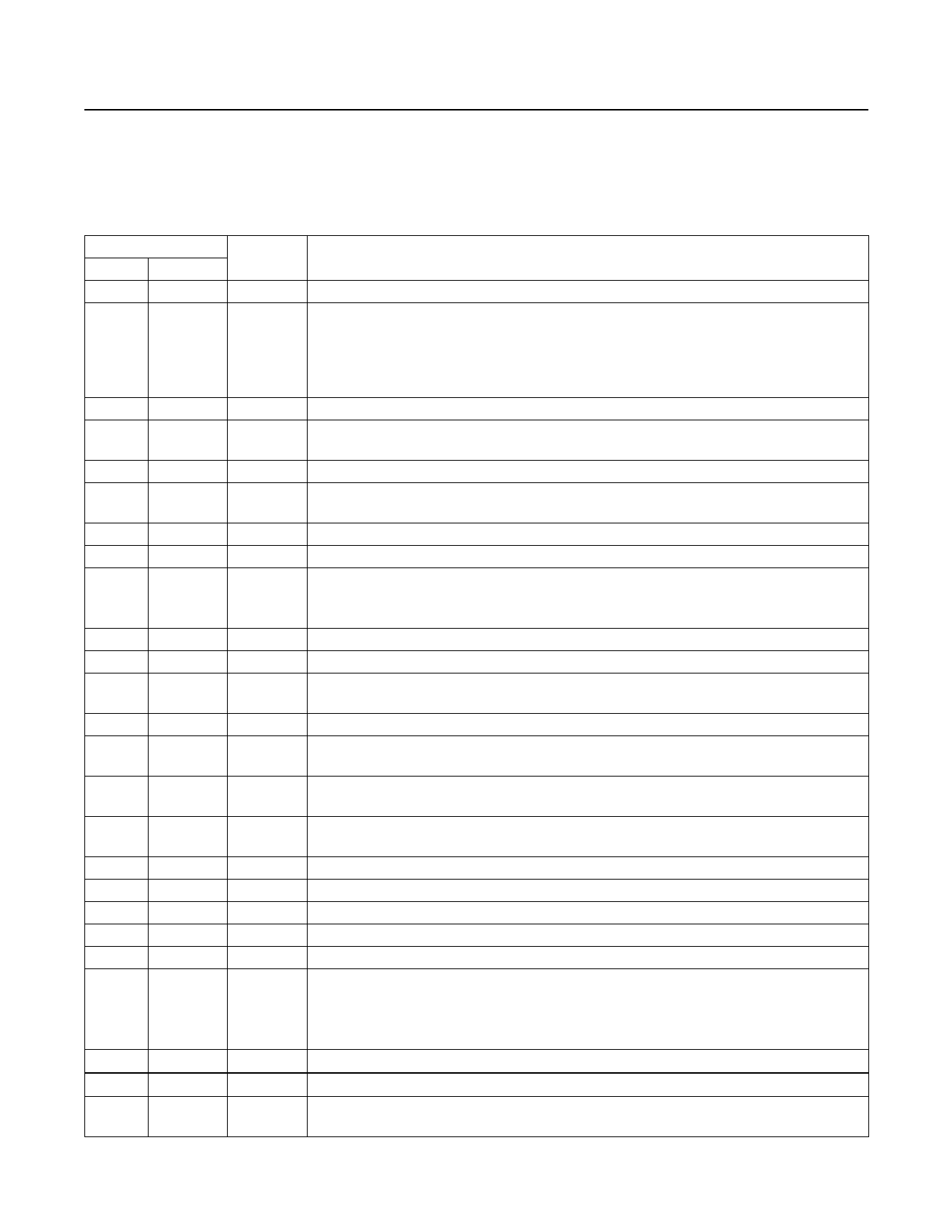
Pin Description
PIN
TSSOP TQFN
1
29
NAME
XTAL1
FUNCTION
Crystal Input 1 (see the Phase-Locked Loop section)
Positive Analog Supply Voltage. For +5V operation, pin 2 is the output of an on-chip +3.2V
low-dropout regulator, and should be bypassed to AGND with a 0.1µF capacitor as close
2, 7
4, 30
AVDD as possible to the pin. Pin 7 must be externally connected to the supply from pin 2, and
bypassed to AGND with a 0.01µF capacitor as close as possible to the pin (see the Voltage
Regulator section and the Typical Application Circuit).
3
4
5, 10
6
8
9
11
31
LNAIN Low-Noise Amplifier Input (see the Low-Noise Amplifier section)
32
LNASRC
Low-Noise Amplifier Source for External Inductive Degeneration. Connect inductor to ground
to set the LNA input impedance (see the Low-Noise Amplifier section).
2, 7
AGND Analog Ground
3
LNAOUT
Low-Noise Amplifier Output. Connect to mixer input through an LC tank filter (see the Low-
Noise Amplifier section).
5
MIXIN1 1st Differential Mixer Input. Connect to LC tank filter from LNAOUT.
6
MIXIN2 2nd Differential Mixer Input. Connect through a 100pF capacitor to VDD3 side of the LC tank.
Image-Rejection Select. Set VIRSEL = 0V to center image rejection at 315MHz. Leave IRSEL
8
IRSEL unconnected to center image rejection at 375MHz. Set VIRSEL = VDD5 to center image
rejection at 433MHz.
12
9
MIXOUT 330Ω Mixer Output. Connect to the input of the 10.7MHz bandpass filter.
13
10
DGND Digital Ground
14
11
DVDD
Positive Digital Supply Voltage. Connect to both of the AVDD pins. Bypass to DGND with a
0.01µF capacitor as close as possible to the pin (see the Typical Application Circuit).
15
12
AC
Automatic Gain Control. See Figure 1. Internally pulled down to AGND with a 100kΩ resistor.
16
14
XTALSEL
Crystal Divider Ratio Select. Drive XTALSEL low to select fLO/fXTAL ratio of 64, or drive
XTALSEL high to select fLO/fXTAL ratio of 32.
17
15
IFIN1
1st Differential Intermediate-Frequency Limiter Amplifier Input. Bypass to AGND with a
1500pF capacitor as close to the pin as possible.
18
16
IFIN2
2nd Differential Intermediate-Frequency Limiter Amplifier Input. Connect to the output of a
10.7MHz bandpass filter.
19
17
DFO Data Filter Output
20
18
DSN Negative Data Slicer Input
21
19
OPP Noninverting Op-Amp Input for the Sallen-Key Data Filter
22
20
DFFB Data-Filter Feedback Node. Input for the feedback of the Sallen-Key data filter.
23
22
DSP Positive Data Slicer Input
+5V Supply Voltage. Bypass to AGND with a 0.01µF capacitor as close as possible to the
24
23
VDD5
pin. For +5V operation, VDD5 is the input to an on-chip voltage regulator whose +3.2V output
appears at the pin 2 AVDD pin (see the Voltage Regulator section and the Typical Application
Circuit).
25
24
DATAOUT Digital Baseband Data Output
26
26
PDOUT Peak-Detector Output
27
27
SHDN
Power-Down Select Input. Drive high to power up the IC. Internally pulled down to AGND with
a 100kΩ resistor.
www.maximintegrated.com
Maxim Integrated │ 8
Share Link: 