MAX7033(2004) Ver la hoja de datos (PDF) - Maxim Integrated
Número de pieza
componentes Descripción
Fabricante
MAX7033 Datasheet PDF : 16 Pages
| |||
315MHz/433MHz ASK Superheterodyne
Receiver with AGC Lock
Pin Description (continued)
PIN
TSSOP THIN QFN
27
27
28
28
—
1, 13, 21,
25
NAME
SHDN
XTAL2
N.C
FUNCTION
Power-Down Select Input. Drive high to power up the IC. Internally pulled down to AGND
with a 100kΩ resistor.
Crystal Input 2. Can also be driven with an external reference oscillator. (See the Crystal
Oscillator section.)
No Connection
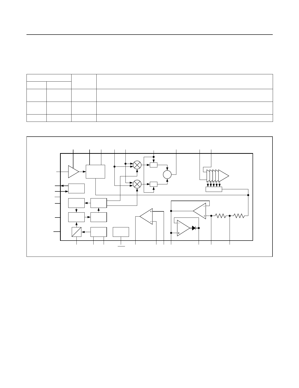
Functional Diagram
LNASRC
4
AC LNAOUT MIXIN1 MIXIN2
15
6
8
9
IRSEL
11
MIXOUT
12
IFIN1 IFIN2
17 18
28-PIN TSSOP
PACKAGE
LNAIN 3
AVDD 2, 7
VDD5 24
AUTOMATIC
LNA
GAIN
CONTROL
3.2V REG
DVDD 14
DIVIDE
BY 64
VCO
DGND 13
PHASE
DETECTOR
LOOP
FILTER
AGND 5, 10
÷1
÷2
16
XTALSEL
CRYSTAL
DRIVER
1 28
XTAL1 XTAL2
0˚
Q
IMAGE
REJECTION
∑
90˚
I
MAX7033
IF LIMITING
AMPS
RSSI
DATA
FILTER
RDF2
RDF1
100kΩ
100kΩ
POWER-
DOWN
DATA
SLICER
27
25
SHDN DATAOUT
20 23 19
DSN DSP DFO
26
21
PDOUT OPP
22
DFFB
Detailed Description
The MAX7033 CMOS superheterodyne receiver and a
few external components provide the complete receive
chain from the antenna to the digital output data.
Depending on signal power and component selection,
data rates as high as 33kbps Manchester (66kbps
NRZ) can be achieved.
The MAX7033 is designed to receive binary ASK data
modulated in the 300MHz to 450MHz frequency range.
ASK modulation uses a difference in amplitude of the
carrier to represent logic 0 and logic 1 data.
Voltage Regulator
For operation with a single +3.0V to +3.6V supply voltage,
connect AVDD, DVDD, and VDD5 to the supply voltage.
For operation with a single +4.5V to +5.5V supply volt-
age, connect VDD5 to the supply voltage. An on-chip
voltage regulator drives one of the AVDD pins to
approximately +3.2V. For proper operation, DVDD and
both AVDD pins must be connected together. Bypass
DVDD and both AVDD pins to AGND with 0.01µF
capacitors placed as close to the pins as possible.
Low-Noise Amplifier
The LNA is an nMOS cascode amplifier with off-chip
inductive degeneration, with a 3.0dB noise figure and
an IIP3 of -12dBm. The gain and noise figures are
dependent on both the antenna matching network at
the LNA input and the LC tank network between the
LNA output and the mixer inputs.
_______________________________________________________________________________________ 9
Share Link: 