MAX6973 Ver la hoja de datos (PDF) - Maxim Integrated
Número de pieza
componentes Descripción
Fabricante
MAX6973 Datasheet PDF : 23 Pages
| |||
16-Output PWM LED Drivers
for Message Boards
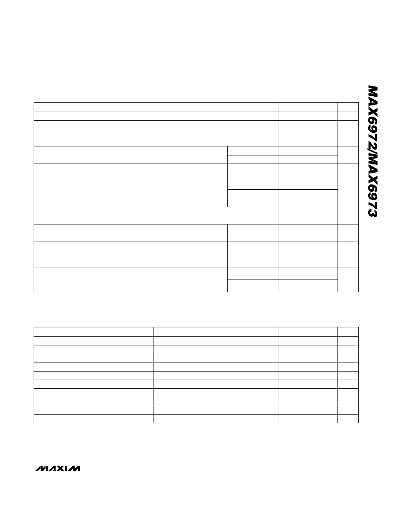
ELECTRICAL CHARACTERISTICS (continued)
(VDD = 3.0V to 3.6V, TA = TMIN to TMAX, unless otherwise noted. Typical values are at VDD = 3.3V, TA = +85°C.) (Note 1)
PARAMETER
Output Low Voltage MUX_
Open-Circuit Detection
Output Slew Time
Y0–Y7, Z0–Z7
Full-Scale Port Output Current
Y0–Y7, Z0–Z7
Port-to-Port Current Matching
Y0–Y7, Z0–Z7
SYMBOL
CONDITIONS
VOLM
VOCD
ISINK = 40mA
80% to 20%, load = 50pF,
calibration DACs set to 0xFF
ISINKFS
VDD = 3.3V, VO = 1.2V,
TA = +85°C
calibration DACs set to 0xFF TA = TMIN to TMAX
∆ISINK
VDD = 3.3V, VO = 1.2V,
calibration DACs set to 0xFF
ISINK = 55mA (Note 2)
TA = +125°C
(Note 3)
TA = +85°C
TA = -40°C
(Note 3)
MIN
54
52.5
TYP MAX UNITS
0.4
V
200
mV
100 ns
55 56
mA
55 58.0
±0.5 ±1.8
±0.5 ±1.2 %
±0.7 ±2.3
Device-to-Device Current Matching
Y0–Y7, Z0–Z7
∆IAVG
VDD = 3.3V, VO = 1.2V, calibration DACs set to 0xFF,
ISINK = 55mA, TA = +85°C (Note 3)
±1 ±2
%
Half-Scale Port Output Current
Y0–Y7, Z0–Z7
ISINKHS
VDD = 3.3V, VO = 1.2V,
calibration DACs set to 0x80
TA = +85°C
TA = TMIN to TMAX
31.0
30.0
33
33
35.5
36.5
mA
Output Load Regulation
∆IOLR
VDD = 3.3V, VO = 1.2V to
3.0V, calibration DACs set to
0x80, ISINK = 33mA
TA = +85°C
TA = TMIN to TMAX
0.3 1.15
mA/V
1.5
Output Power-Supply Rejection
∆IOPSR
VDD = 3.0 V to 3.6V,
VO = 1.2V, calibration DACs
set to 0x80, ISINK = 33mA
TA = +85°C
TA = TMIN to TMAX
0.6 1.7
mA/V
2.0
TIMING CHARACTERISTICS
(VDD = 3.0V to 3.6V, TA = TMIN to TMAX, unless otherwise noted. Typical values are at 3.3V, TA = +85°C.) (Note 1)
PARAMETER
CLKI_ Input Frequency
CLKI_ Duty Cycle
CLKO_ Output Delay
DIN_ Setup Time
DIN_ Hold Time
DOUT_ Output Delay
LOADO Output Delay
LOADI Setup Time
LOADI Hold Time
Watchdog Period
SYMBOL
fCLKI
CONDITIONS
tPD-CLKO
tSU-DIN
tHD-DIN
tPD-DOUT
tPD-LOADO
tSU-LOADI
tHD-LOADI
When enabled
MIN TYP
40
0.5
5
-3
8
40 125
Note 1: All parameters tested at TA = +85°C. Specifications over temperature are guaranteed by design.
Note 2: Specification limits apply to devices at the same TA for TA = TMIN to TMAX.
Note 3: Guaranteed by design.
MAX
33
60
16
15
18
300
UNITS
MHz
%
ns
ns
ns
ns
ns
ns
ns
ms
_______________________________________________________________________________________ 3
Share Link: 