MAX6972 Ver la hoja de datos (PDF) - Maxim Integrated
Número de pieza
componentes Descripción
Fabricante
MAX6972 Datasheet PDF : 23 Pages
| |||
16-Output PWM LED Drivers
for Message Boards
Individual PWM Control
The MAX6972/MAX6973 further modulate the time that
each subframe is ON by a pulse-width modulation
(PWM) value. Each output current driver in the Y and Z
ports has a unique 12-bit (MAX6972) or 14-bit
(MAX6973) PWM control value providing fine resolution
adjustment of average current output. Each bit time of
the PWM corresponds to one period of CLKI (TCLKI).
The PWM setting determines the amount of time (out of
the total period) that the output is on. The subframes
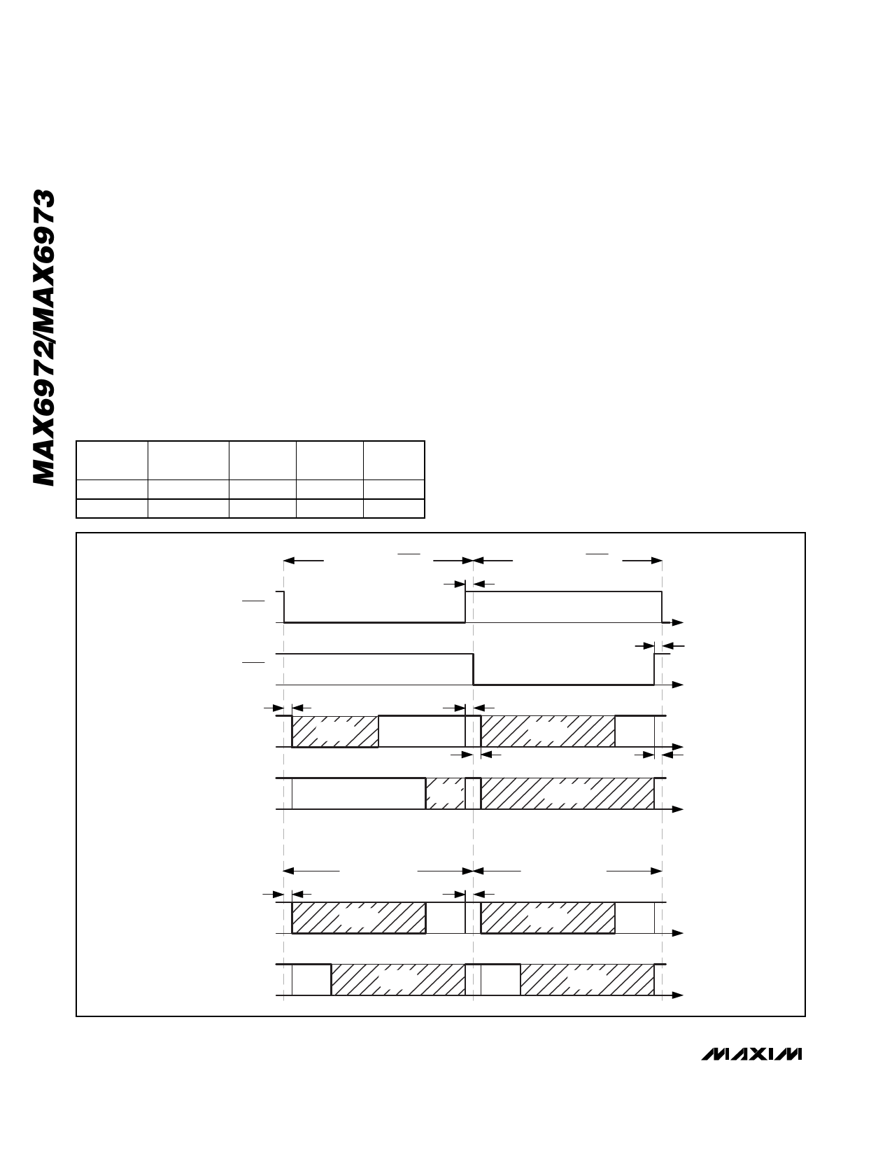
have PWM off zones at the start (tSPWM) and end
(tEPWM) of the PWM period (see Figure 3). The sub-
frame period and PWM off zones are shown in Table 2
for each device.
Table 2. Subframe and PWM Timing
PART
MAX6972
MAX6973
SUBFRAME
(TCLKI)
4096
16,384
tSPWM
(TCLKI)
16
32
tEPWM
(TCLKI)
16
32
tEMUX
(TCLKI)
16
32
MULTIPLEXED
SUBFRAME (n), MUX0
MUX0
MUX1
The MAX6972 subdivides each subframe by 4096
(12-bit) PWM steps and has 16 cycle off zones, leaving
an active PWM region of 4064 PWM steps ranging from
16 to 4079. The MAX6973 subdivides each subframe by
16,384 (14-bit) PWM steps and has 32 cycle off zones,
leaving an active PWM region of 16,320 PWM steps
ranging from 32 to 16,351. The PWM phase for outputs
Y0, Y2, Y4, Y6 and Z0, Z2, Z4, Z6 use phasing with the
outputs on first and off second. Inverse phasing is used
for outputs Y1, Y3, Y5, Y7 and Z1, Z3, Z5, Z7 to balance
the timing of loads on the LED anode power supply, as
shown in Figure 3.
In multiplexed operation, the subframes are shared
between MUX0 and MUX1 active times, effectively
reducing the number of subframes by 2.
LED-Intensity Control Example
The three levels of intensity control are shown in Figure 2
for one LED output driver in a MAX6972 in nonmulti-
plexed mode. As an example, the CALDAC is set to
169DEC, setting the port output current level to 40mA.
SUBFRAME (n), MUX1
tEMUX
tEMUX
Y0, Y2, Y4, Y6
Z0, Z2, Z4, Z6
Y1, Y3, Y5, Y7
Z1, Z3, Z5, Z7
tSPWM
50%
tSPWM
ON/OFF PHASING
25%
OFF/ON PHASING
75%
tSPWM
100%
tEPWM
Y0, Y2, Y4, Y6
Z0, Z2, Z4, Z6
NONMULTIPLEXED
SUBFRAME (n)
tSPWM
tEPWM
75%
ON/OFF PHASING
SUBFRAME (n + 1)
75%
Y1, Y3, Y5, Y7
75%
75%
Z1, Z3, Z5, Z7
OFF/ON PHASING
Figure 3. Multiplexed and Nonmultiplexed Output Driver Phasing and Example PWM Values
10 ______________________________________________________________________________________
Share Link: 