MAX6977 Ver la hoja de datos (PDF) - Maxim Integrated
Número de pieza
componentes Descripción
Fabricante
MAX6977 Datasheet PDF : 13 Pages
| |||
8-Port, 5.5V Constant-Current LED Driver with
LED Fault Detection
The 4-wire serial interface comprises an 8-bit shift reg-
ister and an 8-bit transparent latch. The shift register is
written through a clock input CLK and a data input DIN
and the data propagates to a data output DOUT. The
data output allows multiple drivers to be cascaded and
operated together. The contents of the 8-bit shift regis-
ter are loaded into the transparent latch through a
latch-enable input LE. The latch is transparent to the
shift register outputs when high, and latches the current
state on the falling edge of LE.
Each driver output is an open-drain constant-current
sink that should be connected to the cathode of either
a single LED or a series string of multiple LEDs. The
LED anode can be connected to a supply voltage of up
to 5.5V, independent of the MAX6977 supply, V+. The
constant-current capability is up to 55mA per output,
set for all eight outputs by an external resistor, RSET.
Initial Power-Up and Operation
An internal reset circuit clears the internal registers of
the MAX6977 on power-up. All outputs OUT0 to OUT7,
therefore, initialize high impedance, and the interface
output DOUT initializes low, regardless of the initial
logic levels of the CLK, DIN, OE, and LE inputs.
4-Wire Serial Interface
The serial interface on the MAX6977 is a 4-wire serial
interface using four inputs (DIN, CLK, LE, OE) and a
data output (DOUT). This interface is used to write dis-
play data to the MAX6977. The serial interface data
word length is 8 bits, D0–D7.
The functions of the five interface pins follow. DIN is the
serial-data input, and must be stable when it is sam-
pled on the rising edge of CLK (Table 1). Data is shift-
ed in MSB first. This means that data bit D7 is clocked
in first, followed by 7 more data bits finishing with the
LSB D0.
CLK is the serial clock input, which shifts data at DIN
into the MAX6977 8-bit shift register on its rising edge.
LE is the load input of the MAX6977 latch, which trans-
fers data from the MAX6977 8-bit shift register to its 8-
bit latch when LE is a high (transparent latch), and
latches the data on the LE falling edge of LE (Figure 2).
The rising edge of LE loads fault data into the MAX6977
8-bit shift register, replacing bits D6 and D5 with fault
data. This fault data is automatically shifted out through
DOUT when the next display data is shifted in.
The fourth input provides output enable control of the
output drivers. OE is high to force outputs OUT0 to
OUT7 high impedance, without altering the contents of
the output latches, and low to enable outputs OUT0 to
OUT7 to follow the state of the output latches.
OE is independent of the operation of the serial inter-
face. Data can be shifted into the serial interface shift
register and latched regardless of the state of OE.
DOUT is the serial-data output, which shifts data out
from the MAX6977’s 8-bit shift register on the rising edge
of CLK. Data at DIN is propagated through the shift reg-
ister and appears at DOUT eight clock cycles later.
LED Fault Detection
The MAX6977 includes circuitry that detects open-cir-
cuit LEDs automatically. An open-circuit fault occurs
when an output is programmed to sink current but less
than about 50% of the programmed current flows.
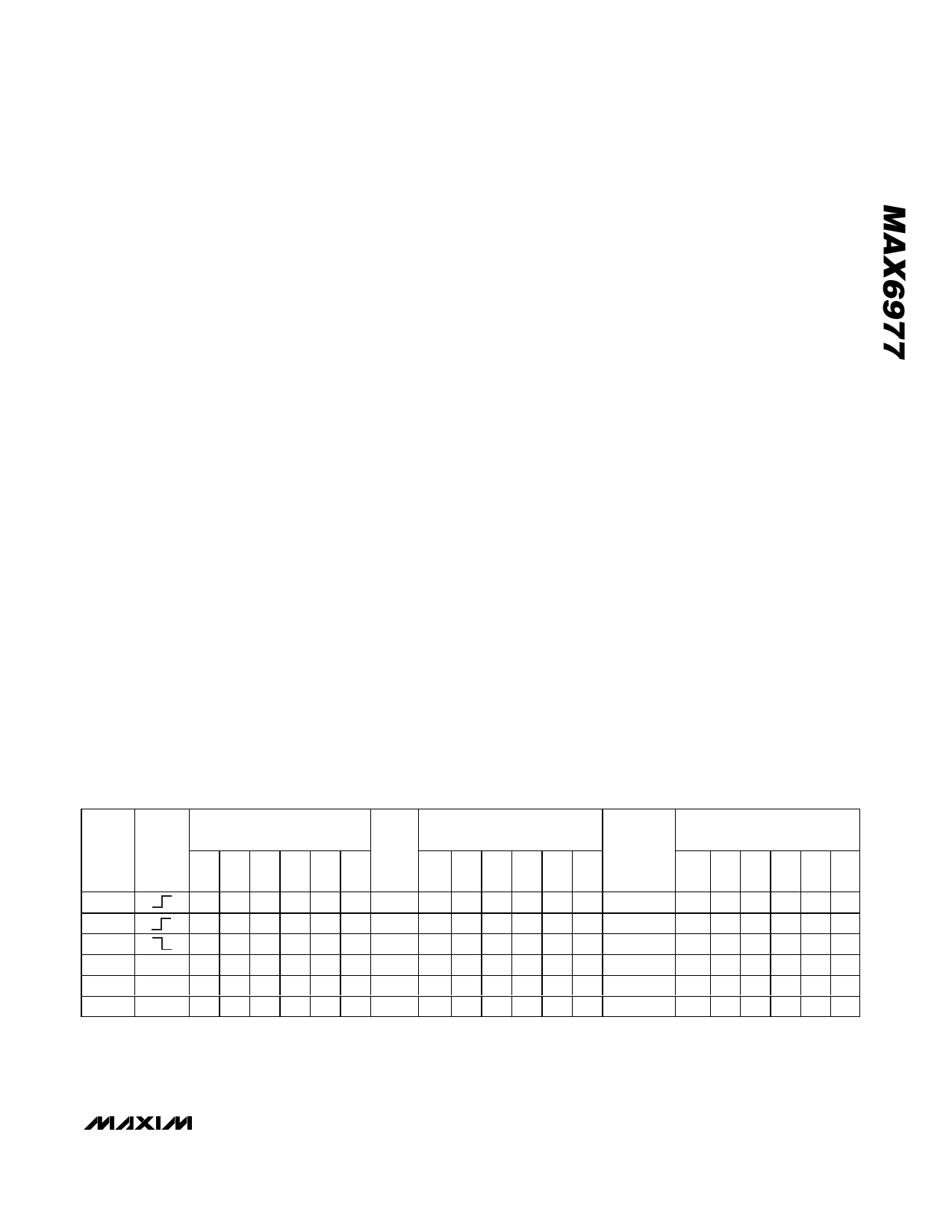
Table 1. 4-Wire Serial Interface Truth Table
SERIAL CLOCK
DATA INPUT
INPUT
DIN CLK D0
SHIFT REGISTER
CONTENTS
LOAD
INPUT
D1 D2 … Dn-1 Dn LE
LATCH CONTENTS
BLANKING
INPUT
D0 D1 D2 … Dn-1 Dn
OE
OUTPUT CONTENTS
D0 D1 D2 … Dn-1 Dn
H
H R1 R2 … Rn-2 Rn-1 — — — — — — —
—
— —————
L
L R1 R2 … Rn-2 Rn-1 — — — — — — —
—
— —————
X
R0 R1 R2 … Rn-1 Rn — — — — — — —
—
— —————
—
—
X X X…X X
H R0 R1 R2 — Rn-1 Rn
—
— —————
—
—
P1 P2 P3 … Pn-1 Pn
L
P0 P1 P2 … Pn-1 Pn
L
P0 P1 P2 … Pn-1 Pn
—
— —————— — X X X … X X
H
Hi-Z Hi-Z Hi-Z … Hi-Z Hi-Z
L = Low-logic level
H = High-logic level
X = Don’t care
P = Present state
R = Previous state
_______________________________________________________________________________________ 7
Share Link: 