MAX3996 Ver la hoja de datos (PDF) - Maxim Integrated
Número de pieza
componentes Descripción
Fabricante
MAX3996 Datasheet PDF : 16 Pages
| |||
3.0V to 5.5V, 2.5Gbps VCSEL
and Laser Driver
ABSOLUTE MAXIMUM RATINGS
Supply Voltage at VCC...........................................-0.5V to +7.0V
Voltage at TX_DISABLE, PORDLY, MON1, COMP,
IN+, IN-, MD, BIAS, MODSET, TC..........-0.5V to (VCC + 0.5V)
Voltage between COMP and MON2 .....................................2.3V
Voltage between IN+ and IN- ..................................................5V
Voltage at OUT+, OUT- .........................(VCC - 2V) to (VCC + 2V)
Voltage between MON1 and MON2 .....................................1.5V
Voltage between BIAS and MON2...........................................4V
Current into FAULT, SHDNDRV ..........................-1mA to +25mA
Current into OUT+, OUT- ....................................................60mA
Current into BIAS ..............................................................120mA
Continuous Power Dissipation (TA = +70°C)
20-Pin QFN (derate 20mW/°C)...................................1600mW
Operating Ambient Temperature Range .............-40°C to +85°C
Operating Junction Temperature Range. ..........-40°C to +150°C
Storage Temperature Range.... .........................-55°C to +150°C
Stresses beyond those listed under “Absolute Maximum Ratings” may cause permanent damage to the device. These are stress ratings only, and functional
operation of the device at these or any other conditions beyond those indicated in the operational sections of the specifications is not implied. Exposure to
absolute maximum rating conditions for extended periods may affect device reliability.
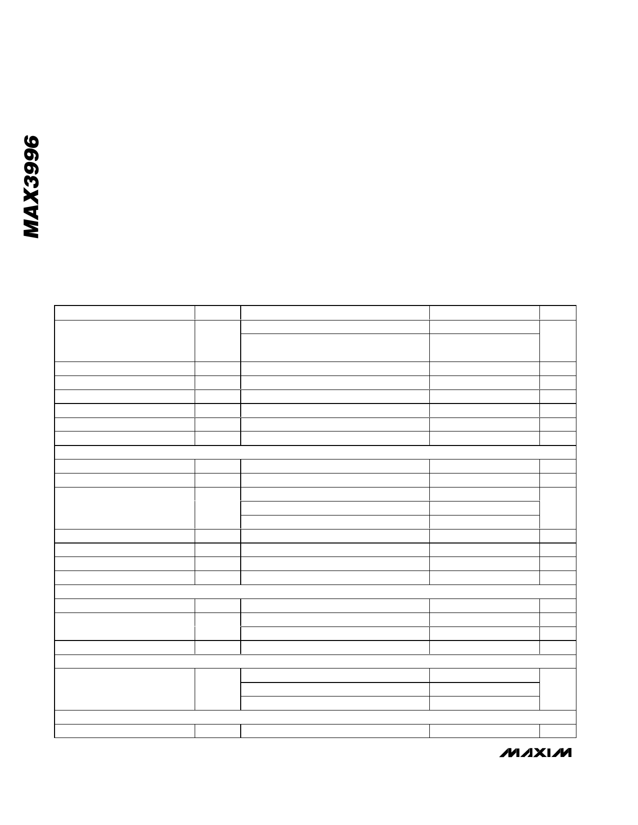
ELECTRICAL CHARACTERISTICS
(VCC = 3.0V to 5.5V, TA = 0°C to +70°C, unless otherwise noted. Typical values are at VCC = 3.3V, TC pin not connected, TA =
+25°C.) (Figure 1)
PARAMETER
SYMBOL
CONDITIONS
MIN TYP MAX UNITS
Supply Current
ICC
(Figure1)
(Note 1)
VCC = 3.3V, IMOD = 15mA
VCC = 5.5V, IMOD = 30mA,
RMODSET = 2.37kΩ
47
mA
52
75
Data Input Voltage Swing
VID
Total differential signal (Figure 2)
TX_DISABLE Input Current
0 < VPIN < VCC
TX_DISABLE Input High Voltage
VIH
TX_DISABLE Input Low Voltage
VIL
FAULT Output High Voltage
VOH
IOH = -100µA, 4.7kΩ < RFAULT < 10kΩ
FAULT Output Low Voltage
VOL
IOL = 1mA
BIAS GENERATOR
200
-100
2.0
2.4
2200
+100
0.8
0.4
mVP-P
µA
V
V
V
V
Minimum Bias Current
Maximum Bias Current
MD Quiescent Voltage
Monitor Resistance
MD Input Current
IBIAS
IBIAS
VMD
RMON
Current into BIAS pin
Current into BIAS pin
APC loop is closed
FAULT = high
TX_DISABLE = high
(Figure 4)
FAULT = low, TX_DISABLE = low
1
mA
60
mA
1.04 1.12
VCC - 0.73
V
VCC - 0.73
9.3
11
12.7
Ω
-3
+0.8
+3
µA
BIAS Current During Fault
APC Time Constant
POWER-ON RESET (POR)
POR Threshold
POR Delay
POR Hysteresis
SHUTDOWN
Voltage at SHDNDRV
LASER MODULATOR
Data Rate
IBIAS_OFF
CCOMP = 0.1µF
tPORDLY
Measured at VCC
PORDLY = open (Note 3)
CPORDLY = 0.001µF (Note 3)
ISHDNDRV = 10µA, FAULT = high
ISHDNDRV = 1mA, FAULT = low
ISHDNDRV = 15mA, FAULT = low
10
µA
35
µs
2.65 2.7
3.0
V
30
55
µs
1.7
2.4
ms
20
mV
VCC - 0.4
0
VCC - 2.4 V
VCC - 1.2
< 3.2
Gbps
2 _______________________________________________________________________________________
Share Link: 