MAX3815 Ver la hoja de datos (PDF) - Maxim Integrated
Número de pieza
componentes Descripción
Fabricante
MAX3815 Datasheet PDF : 11 Pages
| |||
TMDS Digital Video Equalizer for DVI/HDMI
Cables
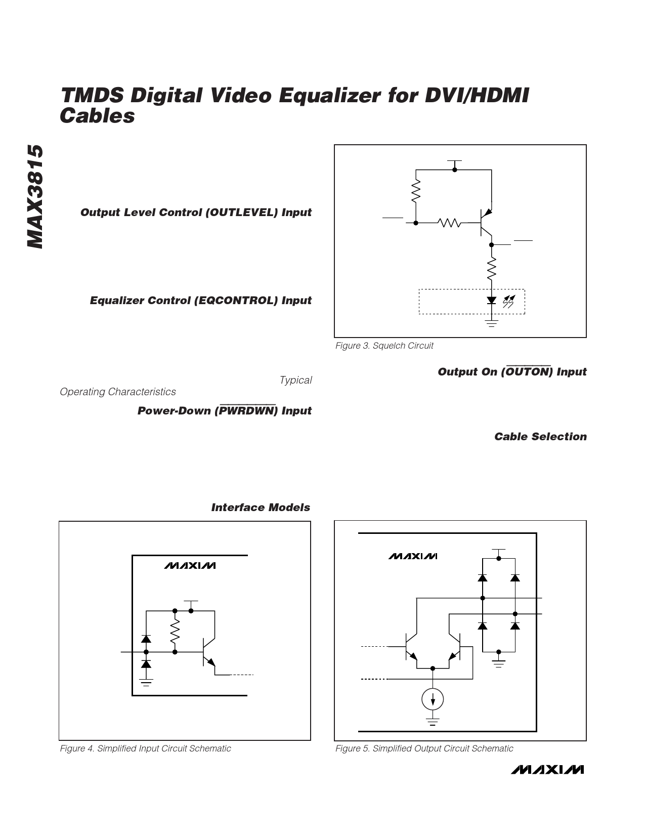
A squelching function can be created by sending the
CLKLOS output through an inverter to the OUTON pin.
This will squelch the CML outputs whenever the clock
signal is removed. A loss-of-signal LED indicator can
be incorporated into the circuit as well (see Figure 3).
Output Level Control (OUTLEVEL) Input
The OUTLEVEL pin is an LVTTL input that allows the
user to select between standard output amplitude
(1000mVP-P differential) or one-half output amplitude
(500mVP-P differential). Forcing this pin high results in
the standard output signal level, and forcing this pin
low results in the reduced output signal level.
Equalizer Control (EQCONTROL) Input
The EQCONTROL pin allows the user to control the
equalization in one of three ways: forcing the pin to
ground sets the equalizer in automatic equalization
mode, forcing the pin to VCC / 2 sets the equalizer to
minimum equalization, and forcing a voltage between
VCC - 1V to VCC allows manual control of the equaliza-
tion level applied to the input signals. See the Typical
Operating Characteristics for more information.
Power-Down (PWRDWN) Input
The PWRDWN pin allows the part to be powered down
to reduce system power consumption. Force the pin
high for normal operation. Force the pin low to power-
down the IC. When powered down, the part consumes
approximately 10mA.
VCC
10kΩ
CLKLOS
4.7kΩ
OUTON
200Ω
LOSS-OF-CLOCK LED
Figure 3. Squelch Circuit
Output On (OUTON) Input
The OUTON pin is an LVTTL input. Force the pin low to
enable the outputs. Force the pin high to set a differential
zero on the outputs. When disabled, the outputs will go to
a differential zero, irrespective of the signal at the inputs.
Cable Selection
TMDS performance is heavily dependent on cable
quality. Deterministic jitter (DJ) can be caused by dif-
ferential-to-common-mode conversion (or vice-versa)
Interface Models
RX_IN+/-
MAX3815
VCC
50Ω
MAX3815
VCC
RX_OUT+
RX_OUT-
Figure 4. Simplified Input Circuit Schematic
Figure 5. Simplified Output Circuit Schematic
8 _______________________________________________________________________________________
Share Link: 