MAX3656 Ver la hoja de datos (PDF) - Maxim Integrated
Número de pieza
componentes Descripción
Fabricante
MAX3656 Datasheet PDF : 16 Pages
| |||
155Mbps to 2.5Gbps Burst-Mode
Laser Driver
loop enters its fine-adjustment mode of operation and
adjusts the bias current to match the level set by the
APCSET resistor. There are three different cases in
which the APC loop starts initialization, and each has a
unique initialization time. These cases are defined
as follows:
• Continuous-Mode Power-Up
In continuous-mode power-up, the chip is enabled
(EN = low) and the burst-enable input is high (BEN =
high) when power is applied to the laser driver. APC
loop initialization begins when the power-supply volt-
age rises above the minimum specified limit of +3.0V.
The BEN input remains high indefinitely and the laser
driver operates in continuous (nonbursting) mode. In
this case, the initialization time is 12µs (typ).
• Chip-Enable Reset
In chip-enable reset, the power-supply voltage is
within the specified limits and BEN is high. The
chip-enable input (EN) is initially high (chip dis-
abled and APC loop reset), and then it is driven low
(chip-enabled). In this case, APC loop initialization
begins when the voltage at EN drops below the
specified EN input low voltage of 0.8V. After initial-
ization begins, the laser driver can be operating in
burst mode (BEN toggling high and low) or continu-
ous mode (BEN = high). In this case, the initializa-
tion time is 2.1µs (typ).
• Burst-Mode Startup
In burst-mode startup, the power-supply voltage is
within the specified limits and the chip is enabled
(EN = low). The burst-enable input is low (BEN =
low) and has not been in the high state since the
APC loop was reset. APC loop initialization begins
when the BEN input is driven high. After initialization
begins, the laser driver can be operating in burst
mode (BEN toggling high and low) or continuous
mode (BEN = high). In this case, the initialization
time is 1.6µs (typ).
In each of the three cases listed, initialization is complete
within three bursts (bursts must comply with specified
burst on- and burst off-time) or the time specified in the
Electrical Characteristics table, whichever comes first.
Burst-Mode Operation
The bias and modulation outputs (BIAS+ and OUT+)
can be switched on and off quickly using the differential
burst-enable inputs (BEN+ and BEN-). Once the APC
loop has initialized, the bias and modulation outputs are
switched on when BEN+ = high and BEN- = low and are
switched off when BEN+ = low and BEN- = high.
When BEN is switched on, the laser driver sinks the bias
and modulation currents set by the APCSET, BIASMAX,
and MODSET resistors within the maximum BEN delay
time of 2.3ns. For stable APC loop operation, the mini-
mum burst length is limited to the burst on-time listed in
the Electrical Characteristics table. The maximum burst-
on time is unlimited.
When BEN is switched off, the bias and modulation cur-
rents fall below the specified bias-off and modulation-
off currents within the maximum burst disable delay
time of 2.0ns. For stable APC loop operation, the mini-
mum burst off-time is limited to the value listed in the
Electrical Characteristics table. The maximum burst off-
time is unlimited.
Short-Circuit Protection
The MAX3656 provides short-circuit protection for the
modulation and bias-current sources. If BIASMAX or
MODSET is shorted to ground, the bias and modulation
outputs are turned off.
Design Procedure
When designing a laser transmitter, the optical output is
usually expressed in terms of average power and
extinction ratio. Table 1 shows the relationships helpful
in converting between the optical average power and
the modulation current. These relationships are valid if
the mark density and duty cycle of the optical wave-
form are 50%.
Programming the Modulation Current
For a given laser power (PAVG), slope efficiency (η),
and extinction ratio (re), the modulation current can be
calculated using Table 1. See the IMOD vs. RMODSET
graph in the Typical Operating Characteristics, and
select the value of RMODSET that corresponds to the
required current at +25°C.
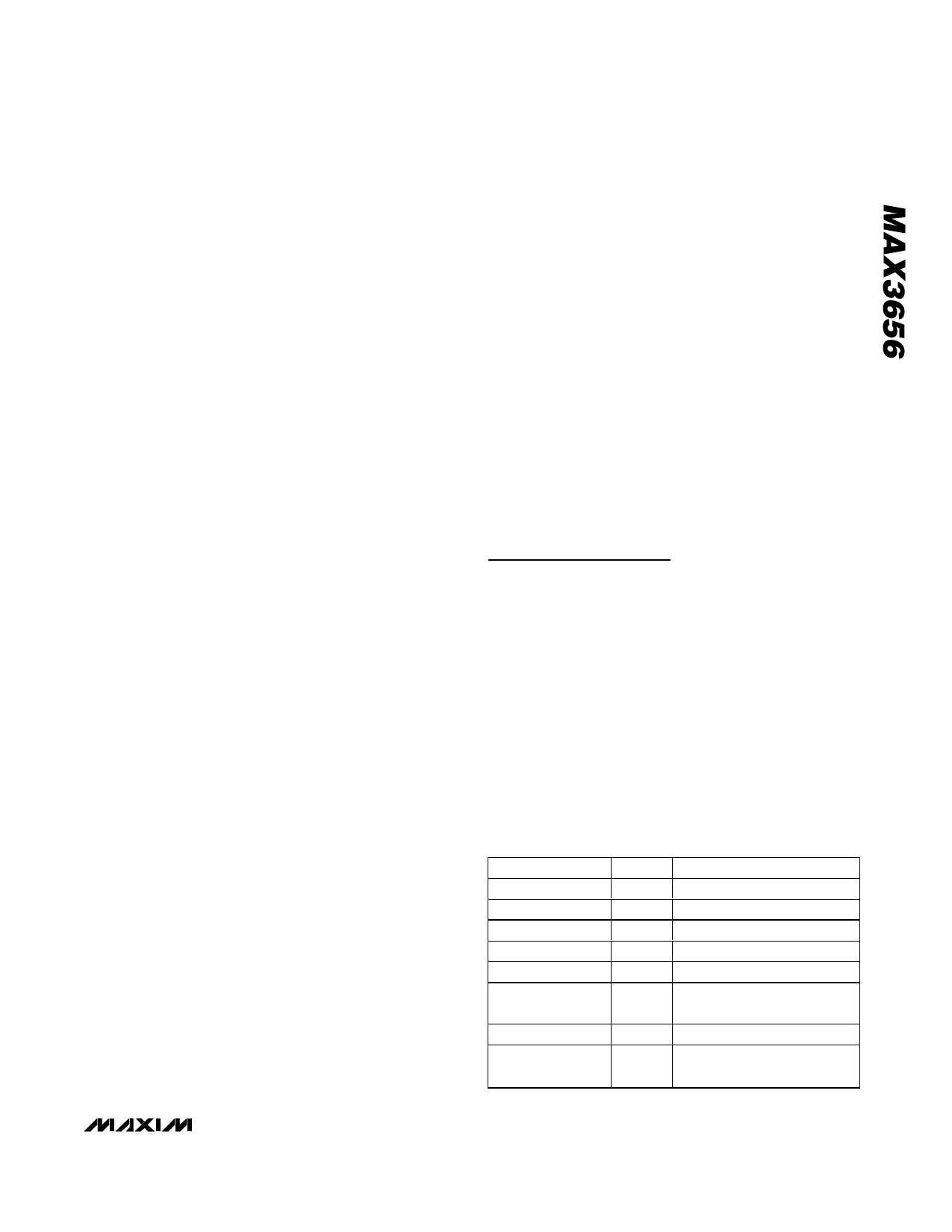
Table 1. Optical Power Definition
PARAMETER SYMBOL
RELATION
Average power
Extinction ratio
Optical power high
Optical power low
Optical amplitude
PAVG
re
P1
P0
PP-P
PAVG = (P0 + P1) / 2
re = P1 / P0
P1 = 2PAVG × re / (re + 1)
P0 = 2PAVG / (re + 1)
PP-P = P1 - P0
Laser slope
efficiency
η
η = PP-P / IMOD
Modulation current IMOD IMOD = PP-P / η
Laser-to-monitor
diode gain
ALMD
(2 x IMD / IMOD)((re - 1) /
(re + 1))
_______________________________________________________________________________________ 9
Share Link: 