MAX3656(2010) Ver la hoja de datos (PDF) - Maxim Integrated
Número de pieza
componentes Descripción
Fabricante
MAX3656 Datasheet PDF : 15 Pages
| |||

155Mbps to 2.5Gbps Burst-Mode
Laser Driver
ABSOLUTE MAXIMUM RATINGS
Supply Voltage, VCC..............................................-0.5V to +6.0V
Current into BIAS+, BIAS-, OUT+, OUT- ........-20mA to +150mA
Current into MD.................................................... -5mA to +5mA
Current into FAIL ...............................................-10mA to +10mA
Voltage at IN+, IN-, BEN+, BEN-, EN,
LONGB ...................................................-0.5V to (VCC + 0.5V)
Voltage at MODSET, APCSET, BIASMAX .............-0.5V to +3.0V
Voltage at OUT+, OUT-.............................+0.5V to (VCC + 1.5V)
Voltage at BIAS+, BIAS-............................+0.5V to (VCC + 0.5V)
Continuous Power Dissipation (TA = +85°C)
24-Lead Thin QFN
(derate 27.8mW/°C above +85°C) .............................1805mW
Operating Ambient Temperature Range (TA)......-40°C to +85°C
Storage Ambient Temperature Range (TSTG) ...-55°C to +150°C
Lead Temperature (soldering,10s) ..................................+300°C
Soldering Temperature (reflow)
Lead(Pb)-free...............................................................+260°C
Containing lead(Pb) .....................................................+240°C
Stresses beyond those listed under “Absolute Maximum Ratings” may cause permanent damage to the device. These are stress ratings only, and functional
operation of the device at these or any other conditions beyond those indicated in the operational sections of the specifications is not implied. Exposure to
absolute maximum rating conditions for extended periods may affect device reliability.
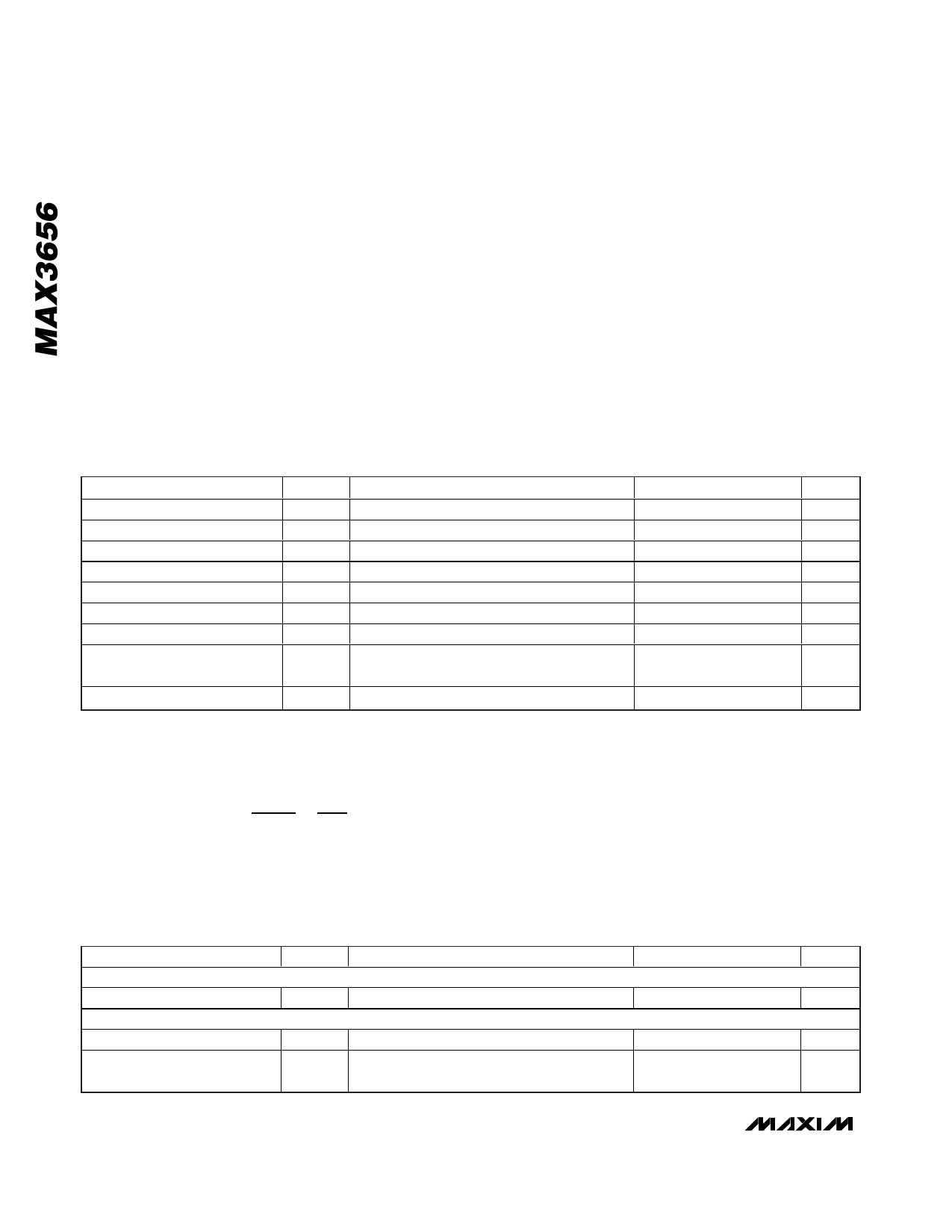
OPERATING CONDITIONS
PARAMETER
SYMBOL
CONDITIONS
MIN TYP MAX UNITS
Supply Voltage
Supply Turn-On Time
VCC
10% to 90%
3.0
3.3
3.6
V
0.001
10
ms
Ambient Temperature
-40
+85
°C
Data Mark Density
Average
50
%
Consecutive Identical Digits
CID
80
Bits
Data Rate
155
2500 Mbps
Monitor Diode Capacitance
CMD For minimum burst on-time (Note 1)
15
pF
Laser-to-Monitor Diode Gain
ALMD
Δ (monitor current)/Δ (laser current (above ITH))
(Notes 2, 3)
0.005
0.050 A/A
Extinction Ratio
re
10 log (P1/P0) (Note 3)
8.2
12.0
dB
Note 1: Larger MD capacitance increases the minimum burst on-time.
Note 2: Laser-to-monitor gain equals the laser slope efficiency multiplied by the photodiode responsivity multiplied by the losses due
to laser-to-monitor diode coupling (ALMD = ηLASER ✕ ρMONITORDIODE ✕ LLASER-TO-MONITORDIODE).
where L = laser-to-monitor diode coupling loss. ALMD can also be calculated by:
ALMD
=
⎛
⎜
⎝
2 × IMD
IMOD
⎞
⎟
⎠
⎛
⎜
⎝
re
re
−
+
I⎞
I⎠⎟
where IMD, IMOD, and re (extinction ratio) are set externally.
Note 3: Operation outside this range degrades APC loop performance.
ELECTRICAL CHARACTERISTICS
(Typical values are at VCC = +3.3V, IBIAS = 20mA, IMOD = 25mA, extinction ratio = 10dB, and TA = +25°C, unless otherwise noted.)
PARAMETER
SYMBOL
CONDITIONS
MIN TYP MAX UNITS
POWER SUPPLY
Power-Supply Current
ICC
(Note 1)
40
70
mA
INPUT SPECIFICATIONS
Differential Input Voltage
VIN, VBEN
0.2
1.6
VP-P
Common-Mode Input Voltage
VCM
VCC -
1.49
VCC -
1.32
VCC -
VIN/4
V
2 _______________________________________________________________________________________