MAX3507 Ver la hoja de datos (PDF) - Maxim Integrated
Número de pieza
componentes Descripción
Fabricante
MAX3507 Datasheet PDF : 12 Pages
| |||
Upstream CATV Amplifier with
On-Chip Anti-Alias Filter
A
G
B
C
DE
F
D7
D6
D5
D4
D3 D2
D1
D0
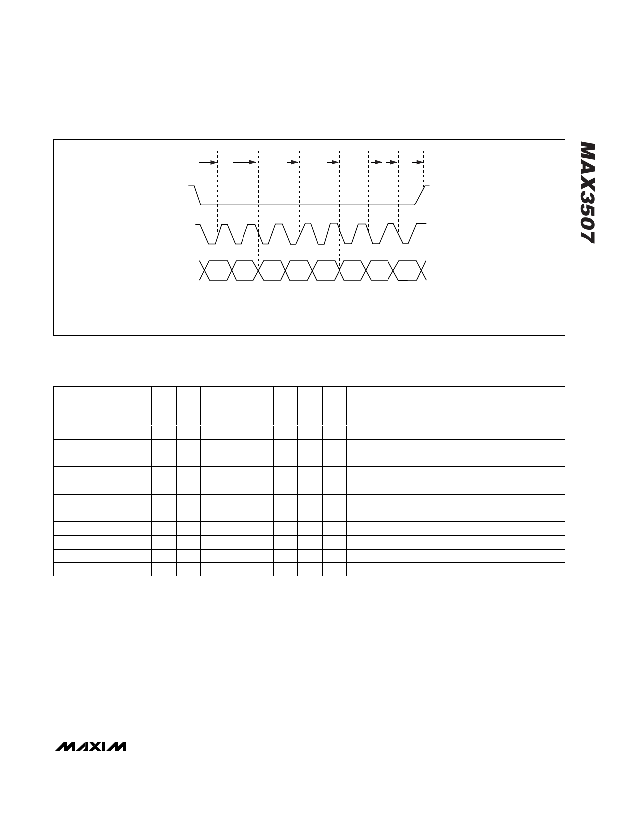
A. tSENS
B. tSDAS
C. tSDAH
D. tSCLKL
E. tSCLKH
F. tSENH
G. tDATAH/tDATAL
Figure 1. Serial Interface Timing Diagram
Table 2. Chip-State Control Bits
SHDN
0
1
TXEN
D7
D6
D5
D4
D3
D2
D1
D0
GAIN STATE
(DECIMAL)
X
XXXXXXXX
—
0
XXXXXXXX
—
1
1
1XXXXXXX
—
GAIN
(dB)
—
—
—
1
1
0XXXXXXX
—
1
1
00110000
48
1
1
01010000
80
1
1
01101110
110
1
1
11010110
86
1
1
11101110
110
1
1
11111101
125
Typical gain at TA = +25°C and VCC = +5V.
—
-22.6
-6.29
8.68
11.69
23.7
31.0
STATES
Shutdown
Transmit Disable Mode
Transmit Enable Mode,
High Power
Transmit Enable Mode,
Low Noise
—
—
—
—
—
—
former must have adequate bandwidth to cover the
intended application. Note that most RF transformers
specify bandwidth with a 50Ω source on the primary
and a matching resistance on the secondary winding.
Operating in a 75Ω system will tend to shift the low-fre-
quency edge of the transformer bandwidth specifica-
tion up by a factor of 1.5, due to primary inductance.
Keep this in mind when specifying a transformer.
Bias to the output stage is provided through the center
tap on the transformer primary. This greatly diminishes
the on/off transients present at the output when switch-
ing between transmit and transmit disable modes.
Commercially available transformers typically have
adequate balance between half-windings to achieve
substantial transient cancellation.
Finally, keep in mind that transformer core inductance
varies proportionally with temperature. If the application
requires low temperature extremes (less than 0°C),
adequate primary inductance must be present to sus-
tain low-frequency output capability as temperatures
_______________________________________________________________________________________ 9
Share Link: 