MAX2371ETC Ver la hoja de datos (PDF) - Maxim Integrated
Número de pieza
componentes Descripción
Fabricante
MAX2371ETC Datasheet PDF : 10 Pages
| |||
LNAs with Step Attenuator and VGA
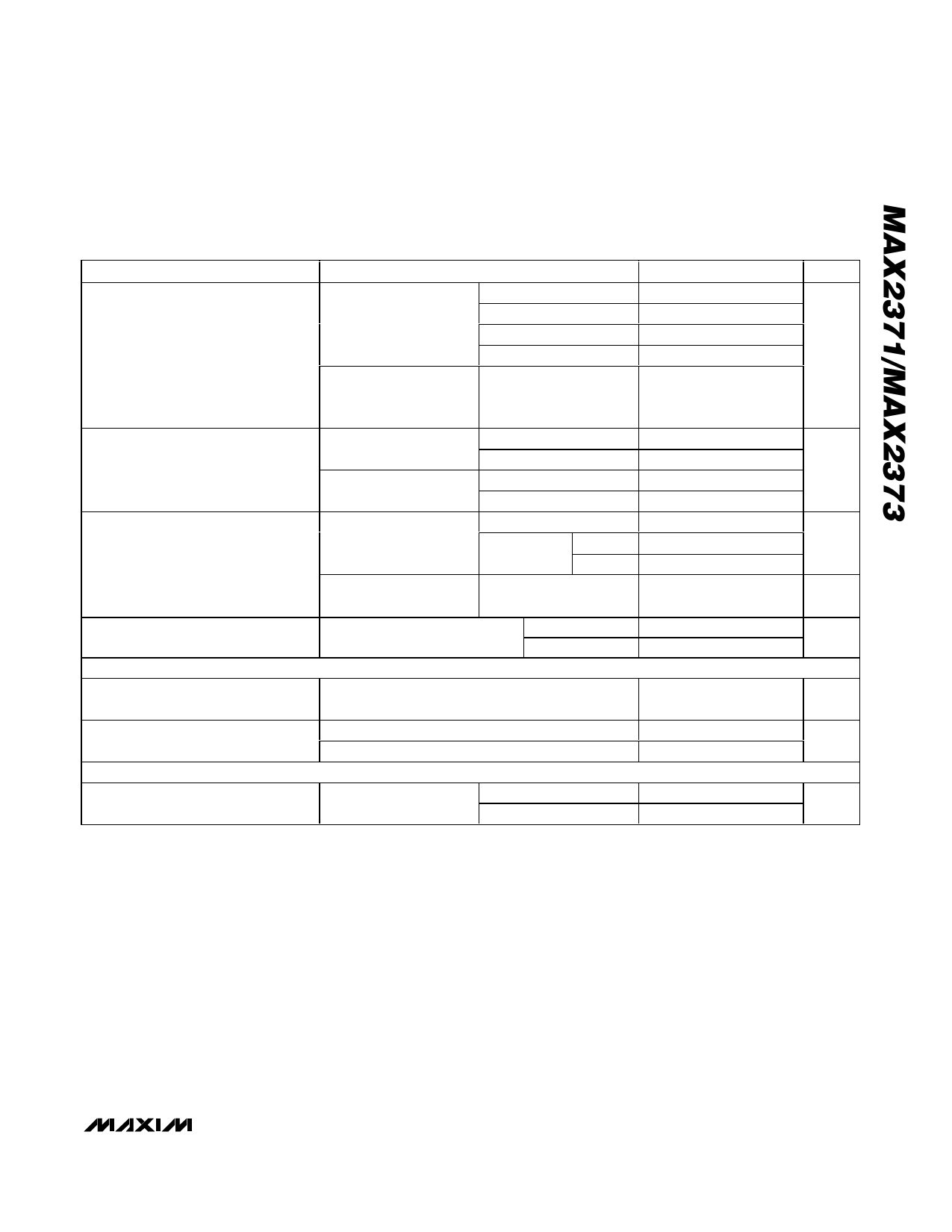
AC ELECTRICAL CHARACTERISTICS (continued)
(MAX2371/MAX2373 EV Kits, VCC = 2.65V to 3.3V, RX_EN = high, RSET = 1.1kΩ, TA = -40°C to +85°C. Typical values are at VCC =
2.775V; for MAX2371 fRF = 150MHz, for MAX2373 fRF = 850MHz to 940MHz; TA = +25°C, unless otherwise noted.) (Note 1)
PARAMETER
SSB Noise Figure vs. AGC
CONDITIONS
LNA_I = high, TA =
+25°C, VCC = 2.775V,
RF_ATTN = low
VAGC = 1.275V
VAGC = 1.575V
VAGC = 1.875V
VAGC = 2.175V
LNA_I = low, TA =
+25°C, VCC = 2.775V,
RF_ATTN = low
VAGC = 1.275V
MIN TYP MAX UNITS
1.8
2.2
5.0
7.7
11
14.5
20
dB
2.1
2.6
Input 1dB Compression Point
Input IP3 (Notes 4, 5)
Input IP3 Over AGC Range
AGC RESPONSE
RF_ATTN = low,
VAGC < 1.8V
LNA_I = high
LNA_I = low
RF_ATTN = high,
VAGC < 1.8V
LNA_I = high
LNA_I = low
RF_ATTN = low,
VAGC = VCC/2
LNA_I = high
MAX2371
LNA_I = low
MAX2373
RF_ATTN = high,
VAGC = VCC/2 to 2.575V LNA_I = high
RF_ATTN = low, LNA_I = high,
VAGC = VCC/2 to 1.80V
MAX2371
MAX2373
-21.5
-24
-3
-9
-5
-7
-12
9
-10.5
-12.5
19.5
-22
0
-6.5
-1
-4
-9
13
-8
-10.5
dBm
dBm
dBm
dBm
AGC Attenuation Range (Note 6)
VCC = 2.775V, RF_ATTN = low, VAGC = 1.3375V
to 2.575V, TA = +25°C
35
45
dB
AGC Slope Over Control Range
RF STEP ATTENUATOR
RF_ATTN = low, VAGC = 1.625V
RF_ATTN = high, VAGC = 1.625V
32
40
47
dB/V
24
33
41
Gain Step
RF_ATTN = high to low, MAX2371
LNA_I = high
MAX2373
16.0 17.5 19.0
dB
18.0 19.5 21.0
Note 1: Parameters over temperature and supply voltage range are guaranteed by design and characterization, unless otherwise noted.
Note 2: Operation outside these frequency bands is possible but has not been characterized. See Typical Operating Characteristics.
Note 3: Measured with external matching network.
Note 4: fIN1 = 150MHz, fIN2 = 150.1MHz, PIN = -30dBm for both tones (MAX2371).
Note 5: fIN1 = 900MHz, fIN2 = 900.1MHz, PIN = -30dBm for both tones (MAX2373).
Note 6: Parameters are guaranteed by production test.
_______________________________________________________________________________________ 3
Share Link: 