MAX2056 Ver la hoja de datos (PDF) - Maxim Integrated
Número de pieza
componentes Descripción
Fabricante
MAX2056 Datasheet PDF : 12 Pages
| |||
800MHz to 1000MHz Variable-Gain
Amplifier with Analog Gain Control
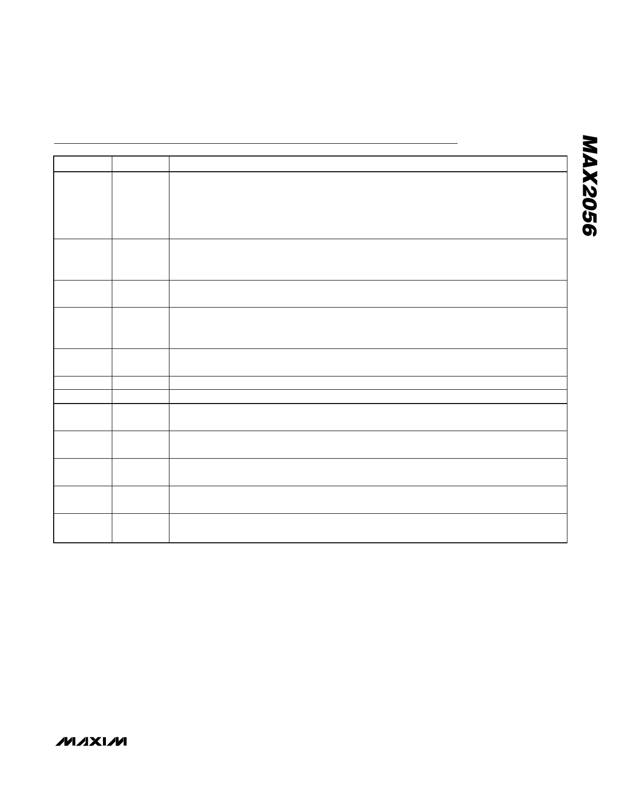
Pin Description
PIN
1, 3, 4, 6, 7,
9, 10, 12, 14,
18, 19,
21–24, 27,
28, 30, 31,
33, 34, 36
2
NAME
GND
OUT_A
FUNCTION
Ground. Connect to the board’s ground plane using low-inductance layout techniques.
Second-Attenuator Output. Internally matched to 50Ω over the operating frequency band. Connect to
IN through a DC-blocking capacitor if greater than 22dB of gain-control range is required. No
connection is required if the second attenuator is not used.
5, 13, 16, 25,
32
VCC
Power Supply. Bypass each pin to GND with capacitors as shown in the Typical Application Circuit.
Place capacitors as close to the pin as possible.
Second-Attenuator Input. Internally matched to 50Ω over the operating frequency band. Connect to a
8
IN_A
50Ω RF source through a DC-blocking capacitor if greater than 22dB of gain-control range is
required. No connection is required if the second attenuator is not used.
11
15
17
20
26
29
35
Exposed
Paddle
VCNTL
RSET1
RSET2
OUT
Analog Gain-Control Input. Limit voltages applied to this pin to a 1V to 4.5V range when VCC is
present to ensure device reliability.
First-Stage Amplifier Bias-Current Setting. Connect to GND through a 1.2kΩ resistor.
Second-Stage Amplifier Bias-Current Setting. Connect to GND through a 3.92kΩ resistor.
RF Output. Internally matched to 50Ω over the operating frequency band. Requires a DC-blocking
capacitor.
AMP_IN Amplifier Input. Internally matched to 50Ω over the operating frequency band. Connect to ATTN_OUT
through a DC-blocking capacitor.
ATTN_OUT Attenuator Output. Internally matched to 50Ω over the operating frequency band. Connect to AMP_IN
through a DC-blocking capacitor.
IN
RF Input. Internally matched to 50Ω over the operating frequency band. Connect to a 50Ω RF source
through a DC-blocking capacitor if the second attenuator is not used.
GND
Exposed Paddle Ground Plane. This paddle affects RF performance and provides heat dissipation.
This paddle MUST be soldered evenly to the board’s ground plane for proper operation.
_______________________________________________________________________________________ 9
Share Link: 