MAX17498A Ver la hoja de datos (PDF) - Maxim Integrated
Número de pieza
componentes Descripción
Fabricante
MAX17498A
Maxim Integrated

MAX17498A Datasheet PDF : 20 Pages
| |||
MAX17498A/MAX17498B/MAX17498C
AC-DC and DC-DC Peak Current-Mode Converters
for Flyback/Boost Applications
Configuring the Power Stage (LX)
The devices use an internal n-channel MOSFET to imple-
ment internal current sensing for current-mode control and
overcurrent protection of the flyback/boost converter. To
facilitate this, the drain of the internal nMOSFET is connect-
ed to the source of the external MOSFET in the MAX17498A
high-input-voltage applications. The gate of the external
MOSFET is connected to the IN pin. Ensure by design that
the IN pin voltage does not exceed the maximum operating
gate-voltage rating of the external MOSFET. The external
MOSFET gate-source voltage is controlled by the switch-
ing action of the internal nMOSFET, while also sensing the
source current of the external MOSFET. In the MAX17498B/
MAX17498C-based applications, the LX pin is directly con-
nected to either the flyback transformer primary winding or
to the boost-converter inductor.
Maximum Duty Cycle
The MAX17498A/MAX17498C operate at a maximum
duty cycle of 94%. The MAX17498B offers a maximum
duty cycle of 92%. The devices can be used to imple-
ment flyback and boost converters involving large input-
to-output voltage ratios in DC-DC applications.
Power-Good Signal (PGOOD)
The devices include a PGOOD signal that serves as
a power-good signal to the system. PGOOD is an
open-drain signal and requires a pullup resistor to the
preferred supply voltage. The PGOOD signal monitors
EA- and pulls high when EA- is 95% (typ) of its regulation
value (1.22V). For isolated power supplies, PGOOD can-
not serve as a power-good signal.
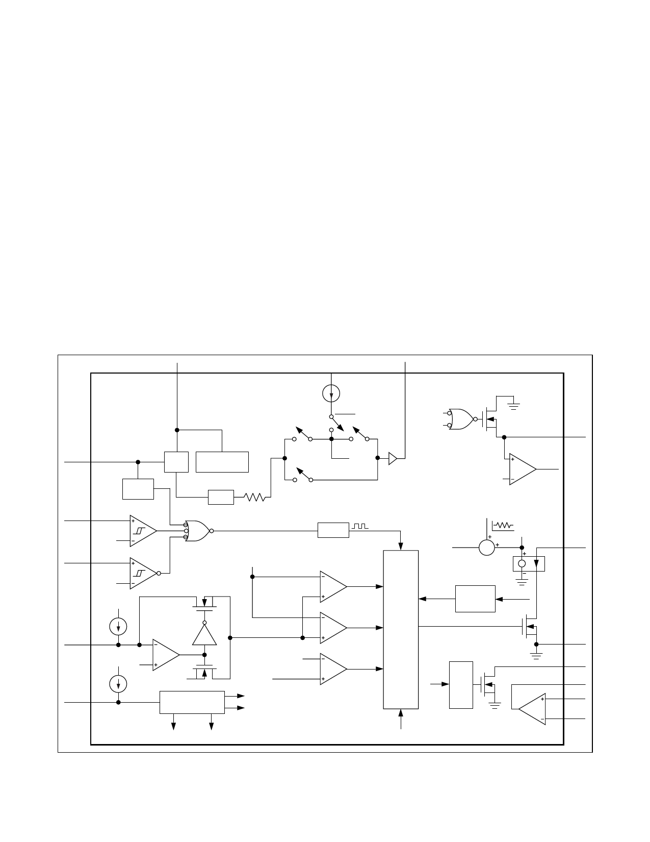
IN
REF
VCC 5V, 50mA
POK
EN/UVLO
1.23V
OVI
1.23V
LDO
33V CLAMP
(MAX17498A ONLY)
BG
VCS
10µA
SSDONE
SSDONE
VOLTAGE SS
CHIPEN
HICCUP
SS
CURRENT SS
MAX17498A
1.17V
MAX17498B
MAX17498C
SS
SSDONEF
CHIPEN
OSC
VSLOPE
VCS
VSUM
LX
CLK
RUNAWAY
SSDONE
1 RUNAWAY
10µA
LIM
10µA
SLOPE
1.23V
250mV
DECODER
LIMINT
VSUM
COMP
FIXED SLOPE
VARIABLE SLOPE
VOLTAGE SS CURRENT SS
PEAK
CONTROL
LOGIC AND
DRIVER
PWM
EA-
PGOOD
BLOCK
CHIPEN
PGND
PGOOD
COMP
EA+
EA-
Figure 1. MAX17498A/MAX17498B/MAX17498C Block Diagram
Maxim Integrated
10
Share Link: