MAX17498A(2012) Ver la hoja de datos (PDF) - Maxim Integrated
Número de pieza
componentes Descripción
Fabricante
MAX17498A
(Rev.:2012)
(Rev.:2012)
Maxim Integrated

MAX17498A Datasheet PDF : 30 Pages
| |||
MAX17498A / MAX17498B / MAX17498C
AC-DC and DC-DC Peak Current-Mode Converters
for Flyback/Boost Applications
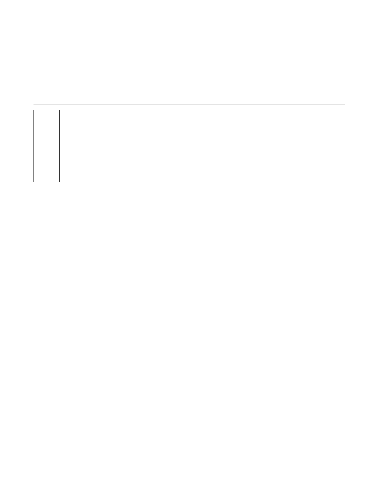
Pin Description (continued)
PIN
NAME
FUNCTION
13
PGOOD
Open-Drain Output. PGOOD goes high when EA- is within 5% of the set point. PGOOD pulls low when
EA- falls below 92% of its set-point value.
14
PGND Power Ground for Converter
15
LX
External Transformer/Inductor Connection for the Converter
16
IN
Internal Linear Regulator Input. Connect IN to the input-voltage source. Bypass IN to PGND with a 1µF
(min) ceramic capacitor.
—
EP
Exposed Pad. Internally connected to SGND. Connect EP to a large copper plane at SGND potential to
(SGND) provide adequate thermal dissipation. Connect EP (SGND) to PGND at a single point.
Detailed Description
The MAX17498A offers a bootstrap UVLO wakeup level
of 20V with a wide hysteresis of 15V (min) optimized
for implementing an isolated and nonisolated universal
(85V AC to 265V AC) offline single-switch flyback
converter or telecom (36V to 72V) power supplies. The
MAX17498B/MAX17498C offer a UVLO wakeup level of
4.4V and are well suited for low-voltage DC-DC flyback/
boost power supplies. An internal reference (1.22V)
can be used to regulate the output down to 1.23V in
nonisolated flyback and boost applications. Additional
semi-regulated outputs, if needed, can be generated
by using additional secondary windings on the flyback
converter transformer. A flexible error amplifier and REF
allow the end-user selection between regulating positive
and negative outputs.
The devices utilize peak current-mode control and exter-
nal compensation for optimizing the loop performance for
various inductors and capacitors. The devices include a
cycle-by-cycle peak current limit and eight consecutive
occurrences of current-limit event trigger hiccup mode,
that protect external components by halting switching for
a period of time (32ms). The devices also include voltage
soft-start for nonisolated designs and current soft-start
for isolated designs to allow monotonic rise of the output
voltage. The voltage or current soft-start can be selected
using the SLOPE pin. See the Block Diagram for more
information.
Input Voltage Range
The MAX17498A has different rising and falling UVLO
thresholds on the IN pin than those of the MAX17498B/
MAX17498C. The thresholds for the MAX17498A are
optimized for implementing power-supply startup
schemes typically used for offline AC-DC power supplies.
The MAX17498A is therefore well suited for opera-
tion from the rectified DC bus in AC-DC power-supply
applications typically encountered in front-end industrial
power-supply applications. As such, the MAX17498A
has no limitation on the maximum input voltage as long
as the external components are rated suitably and the
maximum operating voltages of the MAX17498A are
respected. The MAX17498A can successfully be used
in universal input-rectified (85V to 265V AC) bus applica-
tions, rectified 3-phase DC bus applications, and tele-
com (36V to 72V DC) applications.
The MAX17498B/MAX17498C are intended for imple-
menting a flyback (isolated and nonisolated) and
boost converter with an on-board 65V rated n-channel
MOSFET. The IN pin of the MAX17498B/MAX17498C has
a maximum operating voltage of 36V. The MAX17498B/
MAX17498C implement rising and falling thresholds on
the IN pin that assume power-supply startup schemes,
typical of lower voltage DC-DC applications, down to an
input voltage of 4.5V DC. Therefore, flyback converters
with a 4.5V to 36V supply voltage range can be imple-
mented with the MAX17498B/MAX17498C.
Internal Linear Regulator (VCC)
The internal functions and driver circuits are designed
to operate from a 5V Q5% power-supply voltage. The
devices have an internal linear regulator that is powered
from the IN pin and generates a 5V power rail. The output
of the linear regulator is connected to the VCC pin and
should be decoupled with a 2.2µF capacitor to ground
for stable operation. The VCC converter output supplies
the operating current for the devices. The maximum
operating voltage of the IN pin is 29V for the MAX17498A
and 36V for the MAX17498B/MAX17498C.
���������������������������������������������������������������� Maxim Integrated Products 9
Share Link: