MAX1836 Ver la hoja de datos (PDF) - Maxim Integrated
Número de pieza
componentes Descripción
Fabricante
MAX1836 Datasheet PDF : 15 Pages
| |||
MAX1836/MAX1837
24V Internal Switch, 100% Duty Cycle,
Step-Down Converters
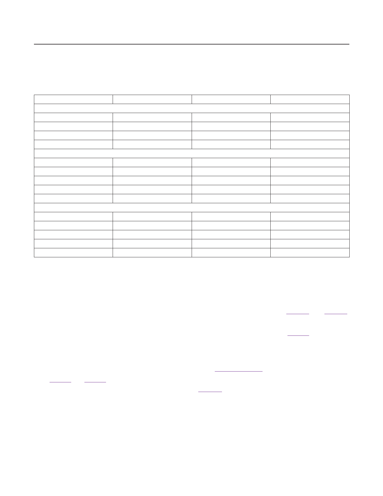
Table 1. Component Suppliers
SUPPLIER
INDUCTORS
Coilcraft
Coiltronics
Sumida USA
Toko
CAPACITORS
AVX
Kemet
Panasonic
Sanyo
Taiyo Yuden
DIODES
Central Semiconductor
International Rectifier
Nihon
On Semiconductor
Zetex
PHONE
847-639-6400
561-241-7876
847-956-0666
847-297-0070
803-946-0690
408-986-0424
847-468-5624
619-661-6835
408-573-4150
516-435-1110
310-322-3331
847-843-7500
602-303-5454
516-543-7100
FAX
847-639-1469
561-241-9339
847-956-0702
847-699-1194
803-626-3123
408-986-1442
847-468-5815
619-661-1055
408-573-4159
516-435-1824
310-322-3332
847-843-2798
602-994-6430
516-864-7630
WEBSITE
www.coilcraft.com
www.coiltronics.com
www.sumida.com
www.tokoam.com
www.avxcorp.com
www.kemet.com
www.panasonic.com
www.secc.co.jp
www.t-yuden.com
www.centralsemi.com
www.irf.com
www.niec.co.jp
www.onsemi.com
www.zetex.com
MAX1836/MAX1837 Stability
Commonly, instability is caused by excessive noise on the
feedback signal or ground due to poor layout or improper
component selection. When seen, instability typically
manifests itself as “motorboating,” which is characterized
by grouped switching pulses with large gaps and exces-
sive low-frequency output ripple during no-load or light-
load conditions.
PC Board Layout and Grounding
High switching frequencies and large peak currents make
PC board layout an important part of the design. Poor lay-
out may introduce switching noise into the feedback path,
resulting in jitter, instability, or degraded performance.
High-power traces, bolded in the typical application cir-
cuits (Figure 1 and Figure 2), should be as short and wide
as possible. Additionally, the current loops formed by the
power components (CIN, COUT, L1, and D1) should be
as tight as possible to avoid radiated noise. Connect the
ground pins of these power components at a common
node in a star-ground configuration. Separate the noisy
traces, such as the LX node, from the feedback network
with grounded copper. Furthermore, keep the extra cop-
per on the board, and integrate it into a pseudoground
plane. When using external feedback, place the resistors
as close to the feedback pin as possible to minimize noise
coupling. The MAX1837 evaluation kit shows the recom-
mended layout.
Applications Information
High-Voltage Step-Down Converter
The typical application circuits’ (Figure 1 and Figure 2)
components were selected for 9V battery applications.
However, the MAX1836/MAX1837 input voltage range
allows supply voltages up to 24V. Figure 6 shows a modi-
fied application circuit for high-voltage applications. When
using higher input voltages, verify that the input capaci-
tor’s voltage rating exceeds VIN(MAX) and that the induc-
tor value exceeds the minimum inductance recommended
in the Inductor Selection section.
Inverter Configuration
Figure 7 shows the MAX1836/MAX1837 in a floating
ground configuration. By connecting what would nor-
mally be the output to the supply-voltage ground, the IC’s
ground pin is forced to regulate to -5V (MAX183_EUT50)
or -3.3V (MAX183_EUT33). Avoid exceeding the maxi-
mum ratings of 24V between IN and GND, and 5.5V
between OUT and GND. Other negative voltages may be
generated by placing a resistive divider across the output
capacitor and connecting the tap to FB in the same man-
ner as the normal step-down configuration.
www.maximintegrated.com
Maxim Integrated │ 11
Share Link: 