MAX1830 Ver la hoja de datos (PDF) - Maxim Integrated
Número de pieza
componentes Descripción
Fabricante
MAX1830 Datasheet PDF : 13 Pages
| |||
3A, 1MHz, Low-Voltage, Step-Down Regulators with
Synchronous Rectification and Internal Switches
Table 2. Output Voltage Programming
PIN
OUTPUT VOLTAGE (V)
FBSEL
FB
MAX1830 MAX1831
VCC
Output voltage
2.5
2.5
Unconnected Output voltage
1.5
1.5
REF
Output voltage
1.8
3.3
GND
Resistive divider
Adjustable
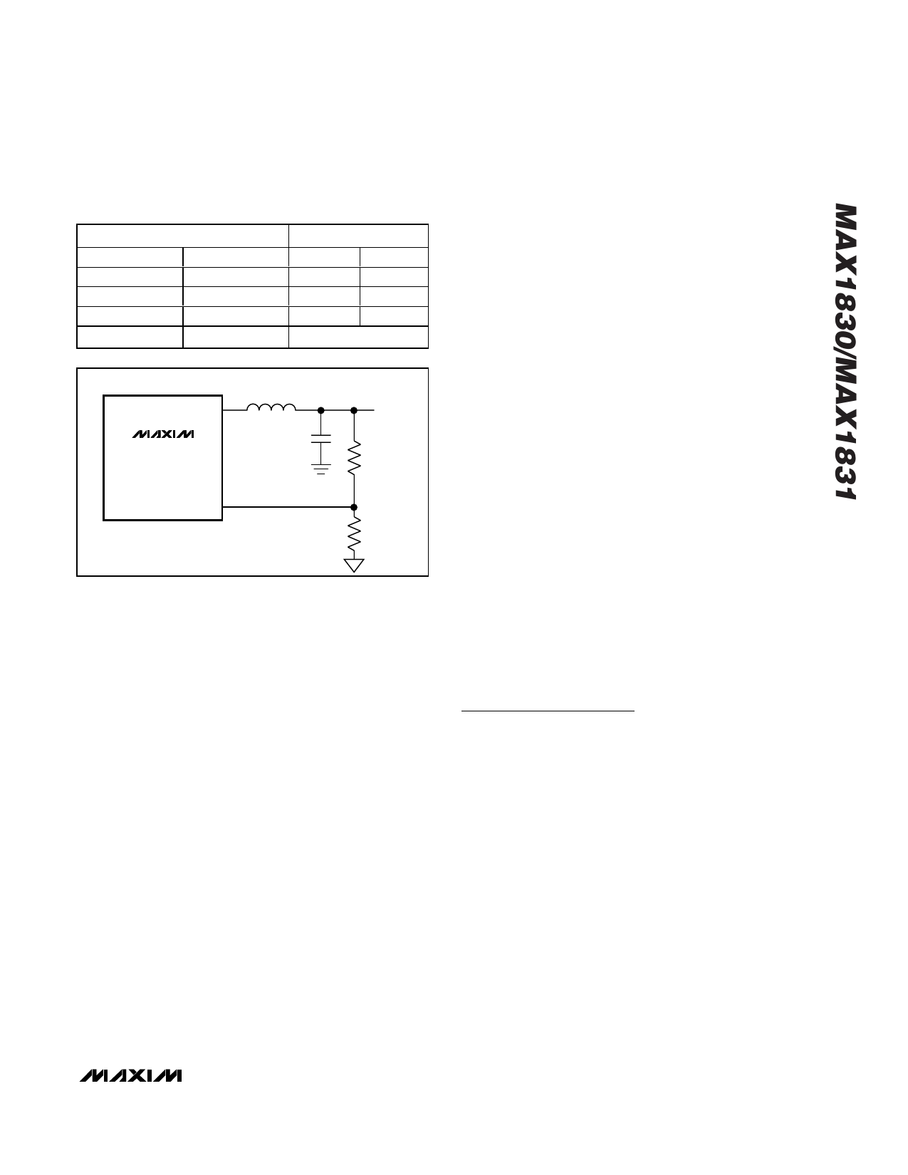
LX
MAX1830
MAX1831
VOUT
R2
FB
R1 = 30kΩ
R1
R2 = R1(VOUT / VREF - 1)
VREF = 1.1V
Figure 4. Adjustable Output Voltage
Synchronous Rectification
In a step-down regulator without synchronous rectifica-
tion, an external Schottky diode provides a path for cur-
rent to flow when the inductor is discharging. Replacing
the Schottky diode with a low-resistance NMOS syn-
chronous switch reduces conduction losses and
improves efficiency.
The NMOS synchronous-rectifier switch turns on follow-
ing a short delay after the PMOS power switch turns off,
thus preventing cross conduction or “shoot through.” In
constant-off-time mode, the synchronous-rectifier
switch turns off just prior to the PMOS power switch
turning on. While both switches are off, inductor current
flows through the internal-body diode of the NMOS
switch. The internal-body diode’s forward voltage is rel-
atively high. An external Schottky diode from PGND to
LX can improve efficiency.
Thermal Resistance
Junction-to-ambient thermal resistance, θJA, is highly
dependent on the amount of copper area immediately
surrounding the IC leads. The MAX1830/MAX1831
evaluation kit has 0.7in2 of copper area and a thermal
resistance of +71°C/W with no forced airflow. Airflow
over the board significantly reduces the junction-to-
ambient thermal resistance. For heatsinking purposes,
evenly distribute the copper area connected at the IC
among the high-current pins.
Power Dissipation
Power dissipation in the MAX1830/MAX1831 is domi-
nated by conduction losses in the two internal power
switches. Power dissipation due to supply current in the
control section and average current used to charge
and discharge the gate capacitance of the internal
switches (i.e., switching losses) is approximately:
PDS = C x VIN2 x fPWM
where C = 5nF and fPWM is the switching frequen-
cy in PWM mode.
This number is reduced when the switching frequency
decreases as the part enters Idle Mode. Combined con-
duction losses in the two power switches are approxi-
mated by:
PD = IOUT2 x RPMOS
where RPMOS is the on-resistance of the PMOS switch.
The junction-to-ambient thermal resistance required to
dissipate this amount of power is calculated by:
where:
θJA = (TJ,MAX - TA,MAX) / PD(TOT)
θJA = junction-to-ambient thermal resistance
TJ,MAX = maximum junction temperature
TA,MAX = maximum ambient temperature
PD(TOT) = total losses
Design Procedure
For typical applications, use the recommended compo-
nent values in Table 1. For other applications, take the
following steps:
1) Select the desired PWM-mode switching frequency;
1MHz is a good starting point. See Figure 3 for maxi-
mum operating frequency.
2) Select the constant off-time as a function of input
voltage, output voltage, and switching frequency.
3) Select RTOFF as a function of off-time.
4) Select the inductor as a function of output voltage,
off-time, and peak-to-peak inductor current.
Setting the Output Voltage
The output of the MAX1830/MAX1831 is selectable
between one of three preset output voltages. For a pre-
set output voltage, connect FB to the output voltage
and connect FBSEL as indicated in Table 2. For an
adjustable output voltage, connect FBSEL to GND and
connect FB to a resistive divider between the output
_______________________________________________________________________________________ 9
Share Link: 