MAX1211 Ver la hoja de datos (PDF) - Maxim Integrated
Número de pieza
componentes Descripción
Fabricante
MAX1211 Datasheet PDF : 30 Pages
| |||
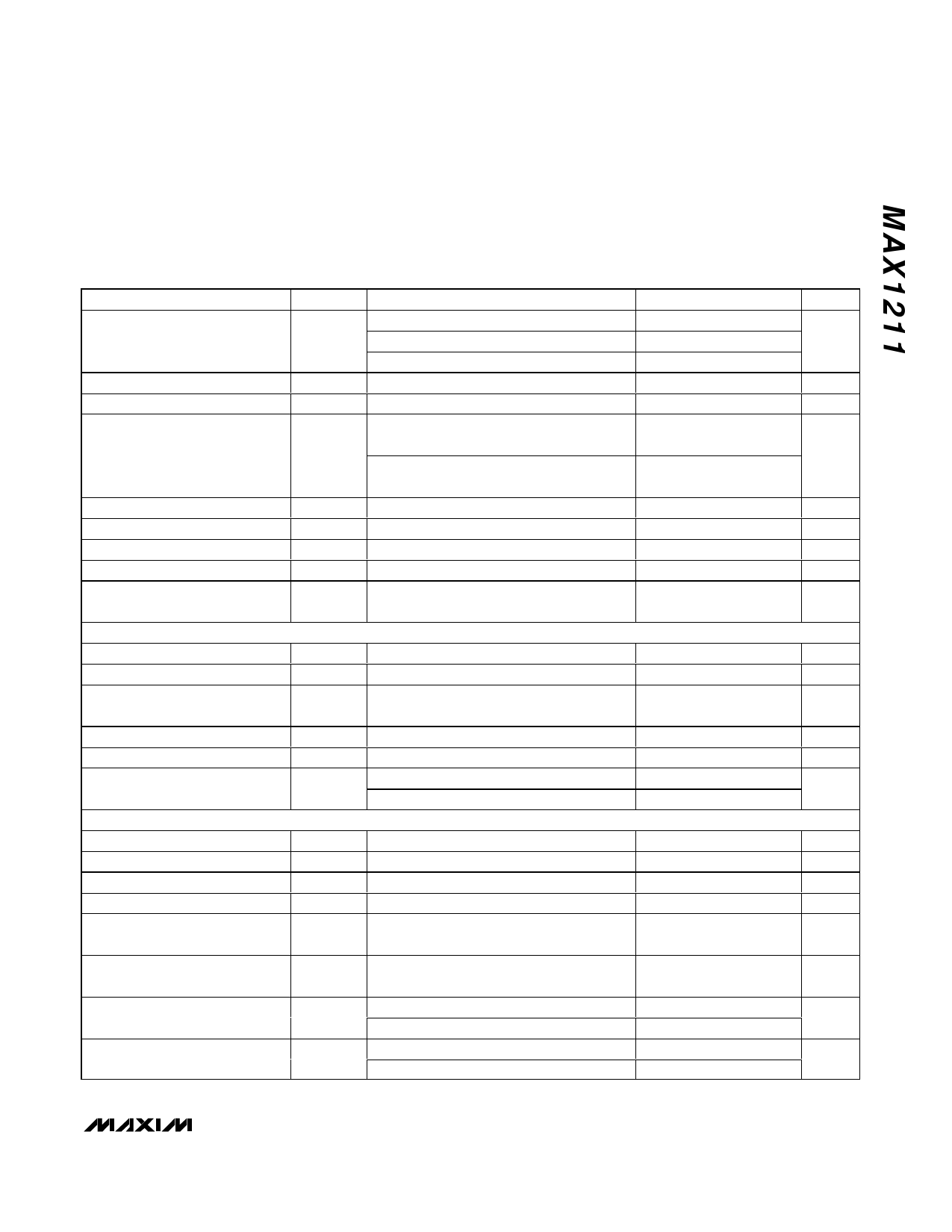
65Msps, 12-Bit, IF Sampling ADC
ELECTRICAL CHARACTERISTICS (continued)
(VDD = 3.3V, OVDD = 2.0V, GND = 0, REFIN = REFOUT (internal reference), CREFOUT = 0.1µF, CL ≈ 5pF at digital outputs, VIN = -
0.5dBFS, CLKTYP = high, DCE = high, PD = low, G/T = low, fCLK = 65MHz (50% duty cycle), CREFP = CREFN = 0.1µF, 1µF in parallel with
10µF between REFP and REFN, CCOM = 0.1µF in parallel with 2.2µF to GND, TA = -40°C to +85°C, unless otherwise noted. Typical values
are at TA = +25°C.) (Note 1)
PARAMETER
SYMBOL
CONDITIONS
MIN TYP MAX UNITS
Total Harmonic Distortion
Second Harmonic
Third Harmonic
THD
HD2
HD3
fIN = 3MHz at -0.5dBFS (Note 3)
fIN = 70MHz at -0.5dBFS (Note 3)
fIN = 175MHz at -5dBFS
fIN1 = 70MHz at -5dBFS
fIN = 70MHz at -0.5dBFS (Note 3)
-89.3 -80.0
-81.3 -73.6 dBc
-78.7 -73.6
-82.4 -74.0 dBc
-90.9 -84.6 dBc
Third-Order Intermodulation
fIN1 = 68.5MHz at -7dBFS
fIN2 = 71.5MHz at -7dBFS
IM3
fIN1 = 172.5MHz at -7dBFS
fIN2 = 177.5MHz at -7dBFS
-82.4
dBc
-81.2
Full-Power Bandwidth
FPBW Input at -0.5dBFS, -3dB rolloff
700
MHz
Aperture Delay
Aperture Jitter
Output Noise
tAD
tAJ
nOUT
Figure 14
Figure 14
INP = INN = COM
0.9
<0.2
0.5
ns
psRMS
LSBRMS
Overdrive Recovery Time
±10% beyond full scale
1
Clock
cycles
INTERNAL REFERENCE (REFIN = REFOUT; VREFP, VREFN, and VCOM are generated internally)
REFOUT Output Voltage
VREFOUT
1.996 2.048 2.071
V
COM Output Voltage
VCOM VDD / 2
1.65
V
Differential Reference Output
Voltage
VREF
VREF = VREFP - VREFN
1.024
V
REFOUT Load Regulation
35
mV/mA
REFOUT Temperature Coefficient TCREF
+100
ppm/°C
REFOUT Short-Circuit Current
Short to VDD
Short to GND
0.24
mA
2.1
BUFFERED EXTERNAL REFERENCE (REFIN driven externally, VREFIN = 2.048V, VREFP, VREFN, and VCOM are generated internally)
REFIN Input Voltage
VREFIN
2.048
V
REFP Output Voltage
REFN Output Voltage
COM Output Voltage
VREFP
VREFN
VCOM
(VDD / 2) + (VREFIN / 4)
(VDD / 2) - (VREFIN / 4)
VDD / 2
2.162
V
1.138
V
1.60 1.65 1.70
V
Differential Reference Output
Voltage
VREF
VREF = VREFP - VREFN
0.978 1.024 1.059
V
Differential Reference
Temperature Coefficient
+12.5
ppm/°C
Maximum REFP Current
Maximum REFN Current
IREFP
IREFN
Source
Sink
Source
Sink
0.4
mA
1.4
1.0
mA
1.0
_______________________________________________________________________________________ 3
Share Link: 