M5M5V408BFP Ver la hoja de datos (PDF) - Renesas Electronics
Número de pieza
componentes Descripción
Fabricante
M5M5V408BFP Datasheet PDF : 10 Pages
| |||
rev. 3.0e, Feb. 12, 2001
M5M5V408BFP,TP,KV
MITSUBISHI LSIs
4194304-BIT (524288-WORD BY 8-BIT) CMOS STATIC RAM
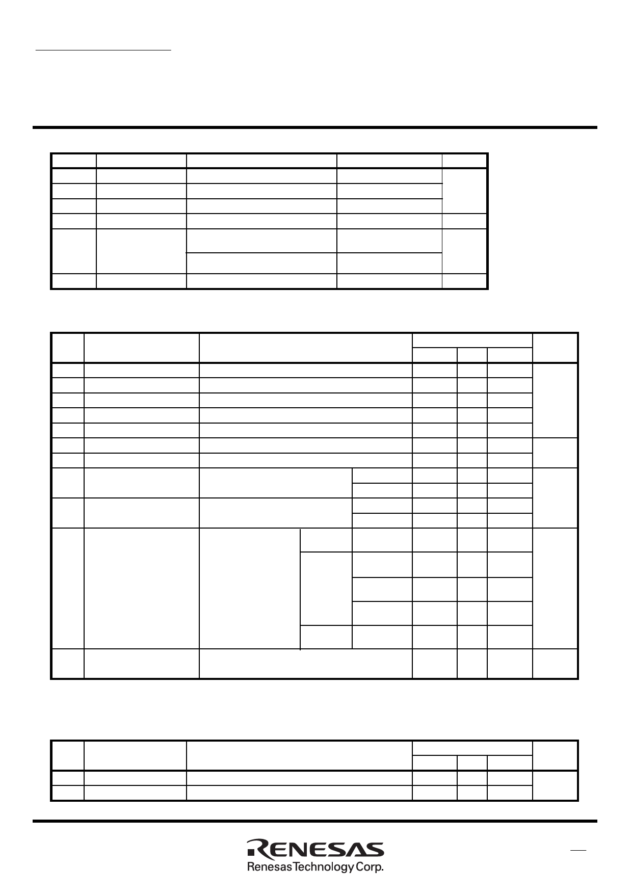
ABSOLUTE MAXIMUM RATINGS
Symbol
Parameter
Conditions
Vcc Supply v oltage
VI
Input v oltage
With respect to GND
With respect to GND
VO Output v oltage
With respect to GND
Pd
Power dissipation
Ta=25°C
Ratings
-0.5* ~ +4.6
-0.5* ~ Vcc + 0.5
0 ~ Vcc
700
Units
V
mW
Operating
Standard (Commercial temp.)
0 ~ 70
Ta
°C
temperature
I-v ersion (Industrial temp.)
- 40 ~ +85
T stg Storage temperature
- 65 ~ +150
°C
* -3.0V in case of AC (Pulse width _< 30ns)
DC ELECTRICAL CHARACTERISTICS
( Vcc=2.7 ~ 3.6V, unless otherwise noted)
Symbol
Parameter
Conditions
VIH
VIL
V OH1
V OH2
V OL
II
IO
High-lev el input v oltage
Low-lev el input v oltage
High-level output voltage 1
High-level output voltage 2
Low-lev el output v oltage
Input leakage current
Output leakage current
IOH= -0.5mA
IOH= -0.05mA
IOL=2mA
VI =0 ~ Vcc
S#=VIH or OE#=VIH, VI/O=0 ~ Vcc
Icc1 Activ e supply c urrent
( AC, CMOS-lev el )
S# <_ 0.2V Output-open
f = 10MHz
Other inputs <_ 0.2V or _> Vcc-0.2V f = 1MHz
Activ e supply c urrent
Icc2 ( AC,TTL-lev el )
S#=VIL Output-open
Other inputs=VIH or VIL
f = 10MHz
f = 1MHz
I-v ersion
85°C
Limits
Min Ty p Max
2.2
Vcc+0.3V
-0.3 *
0.6
2.4
Vcc-0.5V
0.4
±1
±1
-
30 45
-
5
7
-
30 45
-
5
7
-
-
40
Units
V
µA
mA
Vcc=3.6V, max.
70°C
-
-
20
Stand by s upply current
Icc3
(CMOS-lev el input)
S# >_ Vcc-0.2V
I-v ersion,
standard
Other inputs=0~Vcc
40°C
-
1
5
µA
0 ~ +25°C
-
0.3
2
I-v ersion -40 ~ +25°C
-
0.3
2
Icc4 Stand by s upply current
(TTL-lev el input)
S#=VIH ,Other inputs= 0 ~ Vcc
-
-
0.5
mA
* -3.0V in case of AC (Pulse width _< 30ns)
Note 1: Direction f or current f lowing into IC is indicated as positiv e (no mark).
Note 2: Ty pical v alues are sampled at Vcc=3.0V, and are not 100% tested.
CAPACITANCE
Symbol Parameter
CI
Input capacitance
CO Output capacitance
(Vcc=2.7 ~ 3.6V, unless otherwise noted)
Conditions
VI=GND, VI=25mVrms, f =1MHz
VO=GND,VO=25mVrms, f =1MHz
Limits
Min Ty p Max
8
10
Units
pF
3
Share Link: 