M5M5V408BFP Ver la hoja de datos (PDF) - Renesas Electronics
Número de pieza
componentes Descripción
Fabricante
M5M5V408BFP Datasheet PDF : 10 Pages
| |||
rev. 3.0e, Feb. 12, 2001
M5M5V408BFP,TP,KV
MITSUBISHI LSIs
4194304-BIT (524288-WORD BY 8-BIT) CMOS STATIC RAM
FUNCTION
The M5M5408BFP,TP,KV is organized as 524,288-words
by 8-bit. These dev ices operate on a single +2.7~3.6V
power supply , and are directly TTL compatible to both
input and output. Its f ully static circuit needs no clocks
and no ref resh, and makes it usef ul.
A write operation is executed during the S# low and W#
low ov erlap time. The address(A0~A18) must be set up
bef ore the write cy c le
A read operation is executed by s etting W# at a high
lev el and OE# at a low lev el while S# are in an activ e
FUNCTION TABLE
When setting S# at a high lev el, the chips are in a non-
selectable mode in which both reading and writing are
disabled. In this mode, the output stage is in a high-
impedance state, allowing OR-tie with other chips. Setting
the OE# at a high lev el,the output stage is in a high-
impedance state, and the data bus contention problem in
the write cy c le is eliminated.
The power supply c urrent is reduced as low as 0.3µ
A(25°C, ty pical), and the memory data can be held at
+2V power supply , enabling battery back-up operation
during power f ailure or power-down operation in the non-
S# W# OE#
Mode
DQ
Icc
H
X
L
L
L
H
L
H
X Non selection
X Write
L Read
H Read
High-impedance
Data input (D)
Data output (Q)
High-impedance
Standby
Activ e
Activ e
Activ e
note: "H" and "L" in this table mean VIH and VIL, respectiv ely . "X" in this table should be "H" or "L".
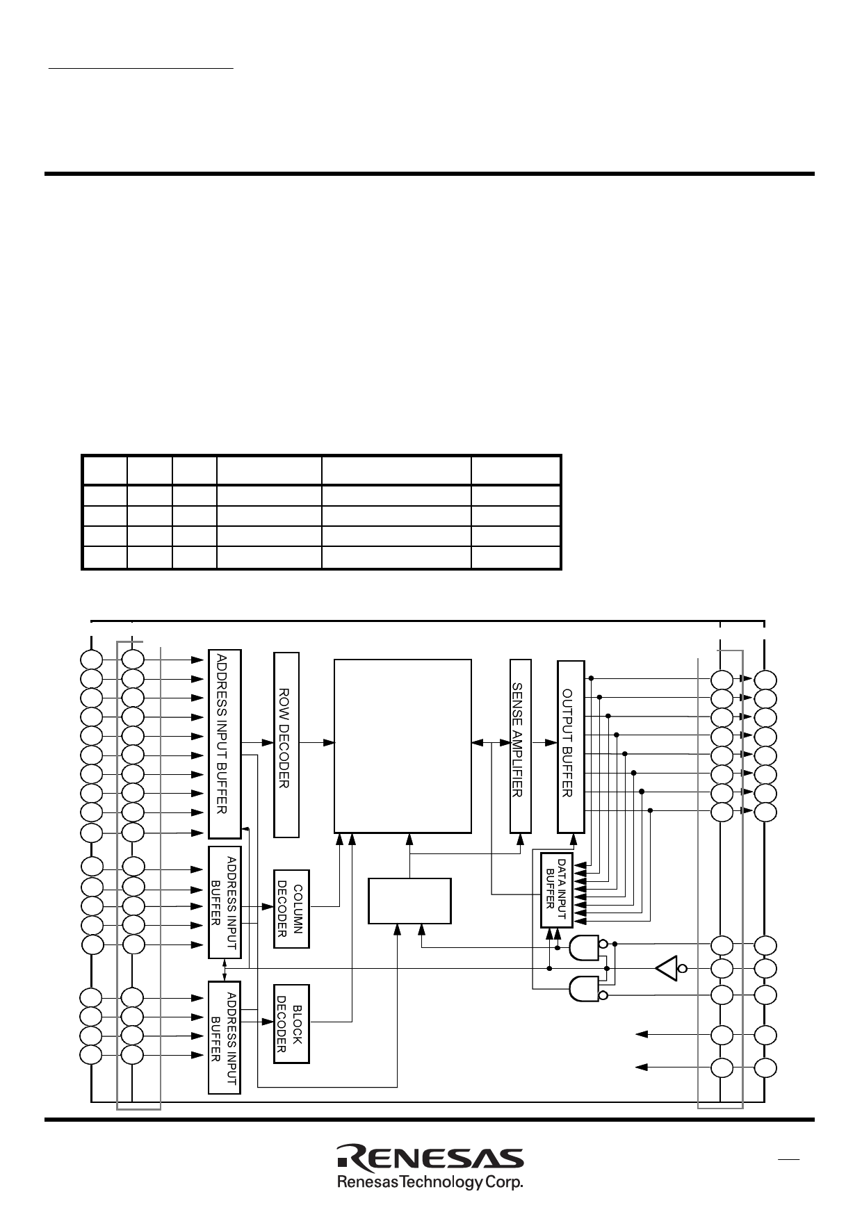
BLOCK DIAGRAM
M5M5V408BFP/TP
M5M5V408BKV
A4 8
16
A5 7
15
A6 6
14
A7 5
13
A12 4
12
A14 3
11
A16 2
10
A17 30
9
A18 1
6
A15 31
7
MEMORY ARRAY
524288 WORDS
x 8 BITS
M5M5V408BFP/TP
M5M5V408BKV
21
13 DQ1
22
14 DQ2
23
15 DQ3
25
17 DQ4
26
18 DQ5
27
19 DQ6
28
20 DQ7
29
21 DQ8
A10 23
31
A11 25
1
A9 26
2
A8 27
3
A13 28
4
A0 12
20
A1 11
19
A2 10
18
A3 9
17
CLOCK
GENERATOR
5
29 W#
30
22 S#
32
24 OE#
8
32 VCC
(3V)
24
16 GND
(0V)
2
Share Link: 