M24M01V-LA6T Ver la hoja de datos (PDF) - STMicroelectronics
NГәmero de pieza
componentes DescripciГіn
Fabricante
M24M01V-LA6T Datasheet PDF : 19 Pages
| |||
M24M01
DEVICE OPERATION
The device supports the I2C protocol. This is sum-
marized in Figure 2. Any device that sends data on
to the bus is defined to be a transmitter, and any
device that reads the data to be a receiver. The
device that controls the data transfer is known as
the bus master, and the other as the slave device.
A data transfer can only be initiated by the bus
master, which will also provide the serial clock for
synchronization. The M24M01 device is always a
slave in all communication.
Start Condition
Start is identified by a falling edge of Serial Data
(SDA) while Serial Clock (SCL) is stable in the
High state. A Start condition must precede any
data transfer command. The device continuously
monitors (except during a Write cycle) Serial Data
(SDA) and Serial Clock (SCL) for a Start condition,
and will not respond unless one is given.
Stop Condition
Stop is identified by a rising edge of Serial Data
(SDA) while Serial Clock (SCL) is stable and driv-
en High. A Stop condition terminates communica-
tion between the device and the bus master. A
Read command that is followed by NoAck can be
followed by a Stop condition to force the device
into the Stand-by mode. A Stop condition at the
end of a Write command triggers the internal EE-
PROM Write cycle.
Acknowledge Bit (ACK)
The acknowledge bit is used to indicate a success-
ful byte transfer. The bus transmitter, whether it be
bus master or slave device, releases Serial Data
(SDA) after sending eight bits of data. During the
9th clock pulse period, the receiver pulls Serial
Data (SDA) Low to acknowledge the receipt of the
eight data bits.
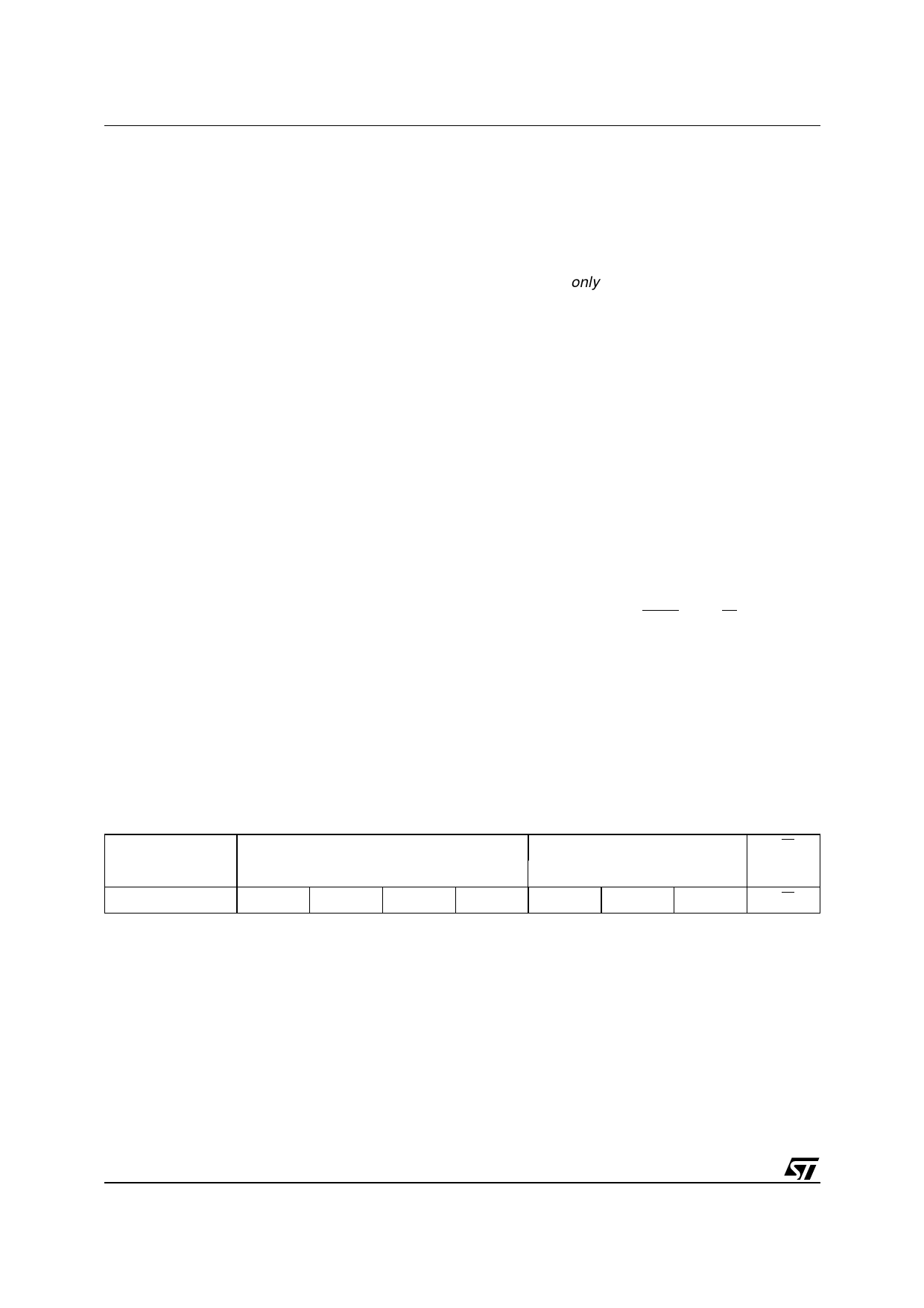
Table 2. Device Select Code 1
Device Type Identifier
b7
b6
b5
Device Select Code
1
0
1
Note: 1. The most significant bit, b7, is sent first.
Data Input
During data input, the device samples Serial Data
(SDA) on the rising edge of Serial Clock (SCL).
For correct device operation, Serial Data (SDA)
must be stable during the rising edge of Serial
Clock (SCL), and the Serial Data (SDA) signal
must change only when Serial Clock (SCL) is driv-
en Low.
Memory Addressing
To start communication between the bus master
and the slave device, the bus master must initiate
a Start condition. Following this, the bus master
sends the Device Select Code, shown in Table 2
(on Serial Data (SDA), most significant bit first).
The Device Select Code consists of a 4-bit Device
Type Identifier, and a 2-bit Chip Enable вҖңAddressвҖқ
(E1, E2). To address the memory array, the 4-bit
Device Type Identifier is 1010b.
Up to four memory devices can be connected on a
single I2C bus. Each one is given a unique 2-bit
code on the Chip Enable (E1, E2) inputs. When
the Device Select Code is received on Serial Data
(SDA), the device only responds if the Chip Enable
Address is the same as the value on the Chip En-
able (E1, E2) inputs.
The 8th bit is the Read/Write bit (RW). This bit is
set to 1 for Read and 0 for Write operations.
If a match occurs on the Device Select code, the
corresponding device gives an acknowledgment
on Serial Data (SDA) during the 9th bit time. If the
device does not match the Device Select code, it
deselects itself from the bus, and goes into Stand-
by mode.
Chip Enable Address
RW
b4
b3
b2
b1
b0
0
E2
E1
A16
RW
4/19
Share Link: 