LX8585-00 Ver la hoja de datos (PDF) - Microsemi Corporation
Número de pieza
componentes Descripción
Fabricante
LX8585-00 Datasheet PDF : 8 Pages
| |||
PRODUCT DATABOOK 1996/1997
LX8585-xx/8585A-xx
4.6A LOW DROPOUT POSITIVE REGULATORS
PRODUCTION DATA SHEET
A B S O L U T E M A X I M U M R AT I N G S (Note 1)
Power Dissipation .................................................................................. Internally Limited
Input Voltage ................................................................................................................ 10V
Input to Output Voltage Differential ........................................................................... 10V
Operating Junction Temperature
Plastic (P, DD Package) ........................................................................................ 150°C
Storage Temperature Range ...................................................................... -65°C to 150°C
Lead Temperature (Soldering, 10 seconds) ............................................................. 300°C
Note 1. Exceeding these ratings could cause damage to the device. All voltages are with respect
to Ground. Currents are positive into, negative out of the specified terminal.
T H E R MAL DATA
P PACKAGE:
THERMAL RESISTANCE-JUNCTION TO TAB, θJT
THERMAL RESISTANCE-JUNCTION TO AMBIENT, θJA
DD PACKAGE:
3.0°C/W
60°C/W
THERMAL RESISTANCE-JUNCTION TO TAB, θJT
3.0°C/W
THERMAL RESISTANCE-JUNCTION TO AMBIENT, θJA
60°C/W*
Junction Temperature Calculation: TJ = TA + (PD x θJA). The θJA numbers are guidelines for the
thermal performance of the device/pc-board system. All of the above assume no ambient airflow.
* θ can be improved with package soldered to 0.5IN2 copper area over backside ground
JA
plane or internal power plane. θJAcan vary from 20ºC/W to > 40ºC/W depending on
mounting technique.
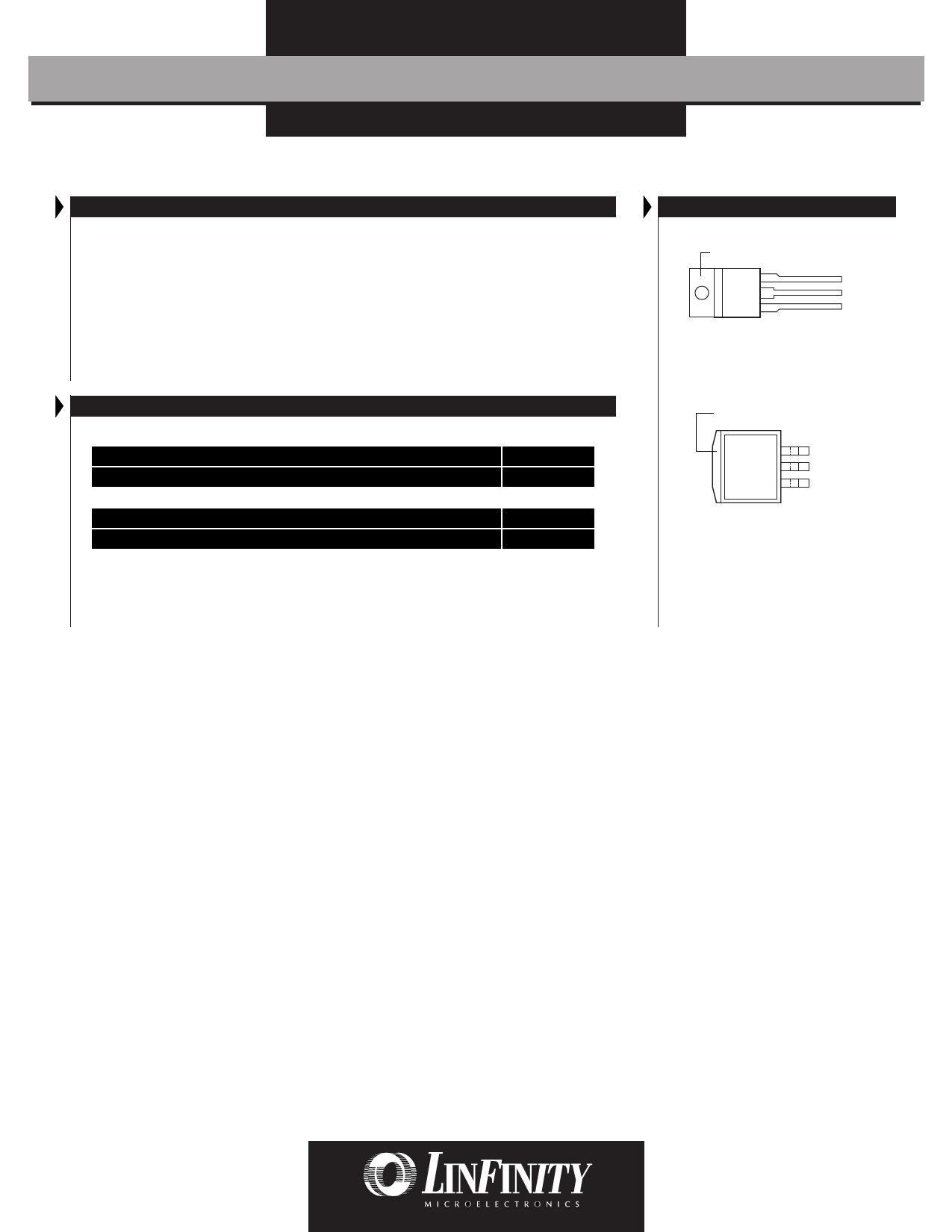
PACKAGE PIN OUTS
TAB IS VOUT
3
2
1
VIN
V
OUT
ADJ / GND*
P PACKAGE
(Top View)
* Pin 1 is GND for fixed voltage versions.
TAB IS VOUT
3
2
1
V
IN
V
OUT
ADJ / GND*
DD PACKAGE
(Top View)
* Pin 1 is GND for fixed voltage versions.
2
Copyright © 1997
Rev. 2.2 12/97
Share Link: 