IS25C01 Ver la hoja de datos (PDF) - Integrated Silicon Solution
Número de pieza
componentes Descripción
Fabricante
IS25C01 Datasheet PDF : 17 Pages
| |||
IS25C01
SERIAL INTERFACE DESCRIPTION
MASTER: The device that provides a clock signal.
SLAVE: The IS25C01 is a slave because the clock
signal is an input.
TRANSMITTER/RECEIVER: The IS25C01 has both data
input (SI) and data output (SO).
MSB: The most significant bit. It is always the first bit
transmitted or received.
OP-CODE: The first byte transmitted to the slave
following CS transition to LOW. If the OP-CODE is a
valid member of the IS25C01 instruction set (Table 3),
then it is decoded appropriately. If the OP-CODE is not
valid, and the SO pin remains in high impedance.
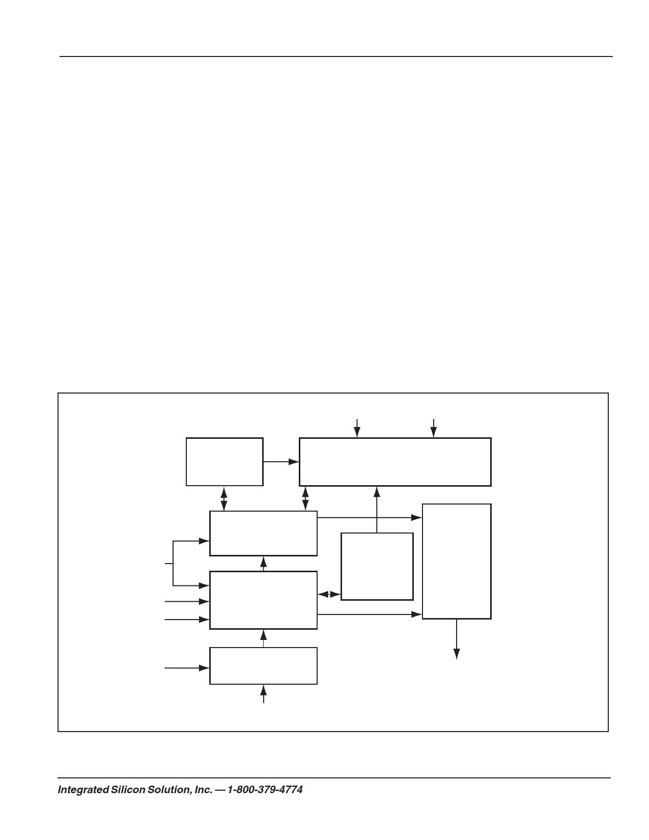
BLOCK DIAGRAM
STATUS
REGISTER
VCC
GND
128 x 8
MEMORY ARRAY
SI
CS
WP
SCK
DATA
REGISTER
MODE
DECODE
LOGIC
CLOCK
HOLD
ADDRESS
DECODER
OUTPUT
BUFFER
SO
ISSI ®
Integrated Silicon Solution, Inc. — 1-800-379-4774
3
Preliminary Information Rev. 00B
12/23/05
Share Link: 