IDT72401(2005) Ver la hoja de datos (PDF) - Integrated Device Technology
Número de pieza
componentes Descripción
Fabricante
IDT72401 Datasheet PDF : 9 Pages
| |||
IDT72401/72403
CMOS PARALLEL FIFO 64 x 4, 64 x 5
MILITARY AND COMMERCIAL
TEMPERATURE RANGES
FUNCTIONAL DESCRIPTION
The 64 x 4 FIFO is designed using a dual port RAM architecture as opposed
to the traditional shift register approach. This FIFO architecture has a write
pointer, a read pointer and control logic, which allow simultaneous read and
write operations. The write pointer is incremented by the falling edge of the Shift
In (Sl) control; the read pointer is incremented by the falling edge of the Shift Out
(SO). The Input Ready (IR) signals when the FIFO has an available memory
location; Output Ready (OR) signals when there is valid data on the output.
Output Enable (OE) provides the capability of three-stating the FIFO outputs.
FIFO RESET
The FIFO must be reset upon power up using the Master Reset (MR) signal.
This causes the FlFO to enter an empty state, signified by Output Ready (OR)
being LOW and Input Ready (IR) being HIGH. In this state, the data outputs
(Q0-3) will be LOW.
DATA INPUT
Data is shifted in on the LOW-to-HlGH transition of Shift In (Sl). This loads
input data into the first word location of the FIFO and causes Input Ready (IR)
to go LOW. On the HlGH-to-LOW transition of SI, the write pointer is moved to
the next word position and IR goes HIGH, indicating the readiness to accept new
data. If the FIFO is full, IR will remain LOW until a word of data is shifted out.
DATA OUTPUT
Data is shifted out on the HlGH-to-LOW transition of Shift Out (SO). This causes
the internal read pointer to be advanced to the next word location. If data is
present, valid data will appear on the outputs and Output Ready (OR) will go
HIGH. If data is not present, OR will stay LOW indicating the FIFO is empty. The
last valid word read from the FIFO will remain at the FlFOs output when it is empty.
When the FIFO is not empty, OR goes LOW on the LOW-to-HIGH transition of
SO. Previous data remains on the output until the HIGH-to-LOW transition of
SO).
FALL THROUGH MODE
The FIFO operates in a fall-through mode when data gets shifted into an empty
FIFO. After a fall-through delay the data propagates to the output. When the
data reaches the output, the Output Ready (OR) goes HIGH. Fall-through mode
also occurs when the FIFO is completely full. When data is shifted out of the full
FIFO, a location is available for new data. After a fall-through delay, the Input
Ready (IR) goes HIGH. If Shift In (SI) is HIGH, the new data can be written
to the FIFO.
Since these FlFOs are based on an internal dual-port RAM architecture with
separate read and write pointers, the fall-through time (tPT) is one cycle long.
A word may be written into the FIFO on a clock cycle and can be accessed on
the next clock cycle.
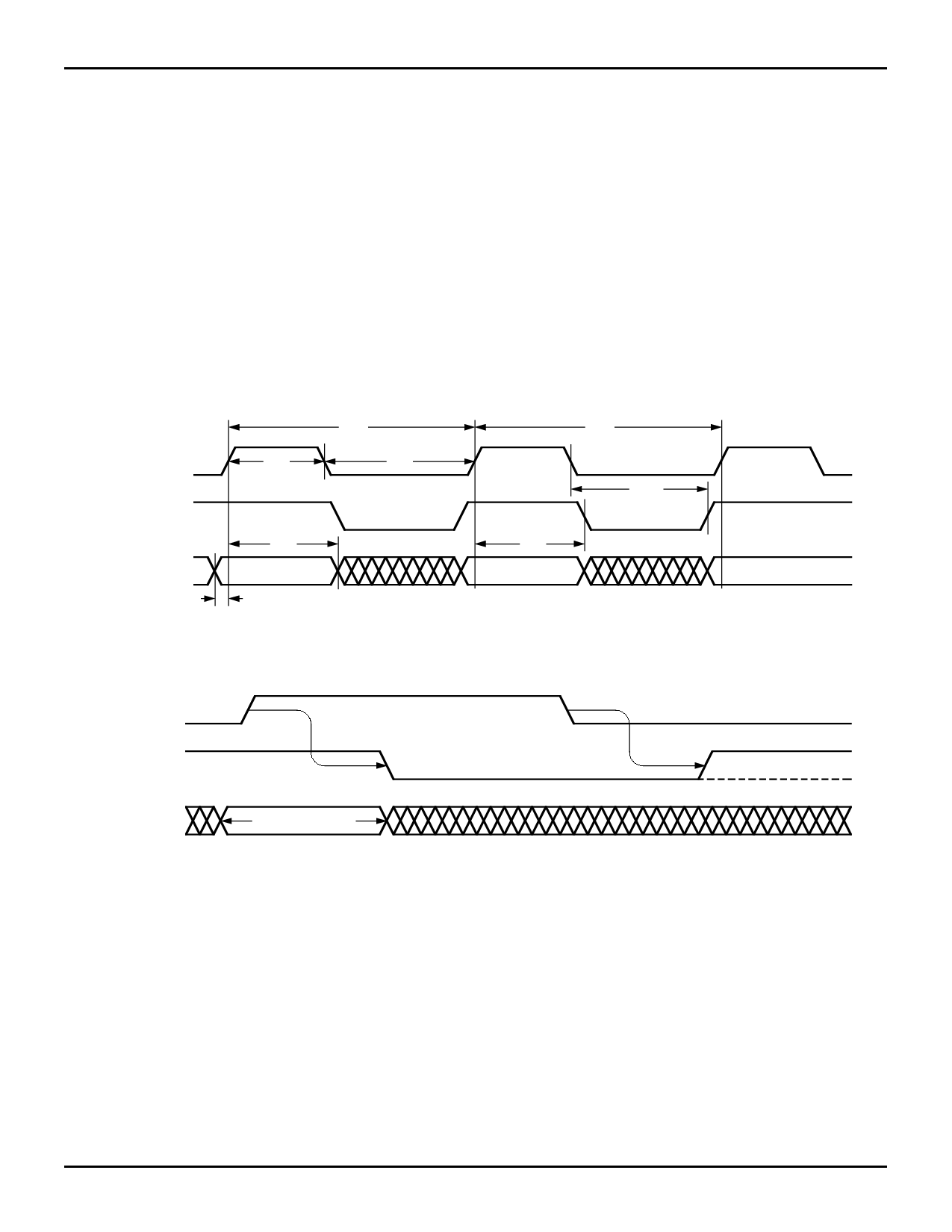
SI
IR
tIDS
INPUT DATA
1/fIN
tSIH
tSIL
tIDH
1/fIN
tIRH
tIRL
Figure 2. Input Timing
SI (7)
(2)
(4)
(1)
IR
(3)
INPUT DATA
STABLE DATA
NOTES:
1. IR HIGH indicates space is available and a SI pulse may be applied.
2. Input Data is loaded into the first word.
3. IR goes LOW indicating the first word is full.
4. The write pointer is incremented.
5. The FIFO is ready for the next word.
6. If the FIFO is full then the IR remains LOW.
7. SI pulses applied while IR is LOW will be ignored (see Figure 4).
Figure 3. The Mechanism of Shifting Data Into the FIFO
5
2747 drw 06
(5)
(6)
2747 drw 07
Share Link: 