IDT72401(2005) Ver la hoja de datos (PDF) - Integrated Device Technology
Número de pieza
componentes Descripción
Fabricante
IDT72401 Datasheet PDF : 9 Pages
| |||
IDT72401/72403
CMOS PARALLEL FIFO 64 x 4, 64 x 5
MILITARY AND COMMERCIAL
TEMPERATURE RANGES
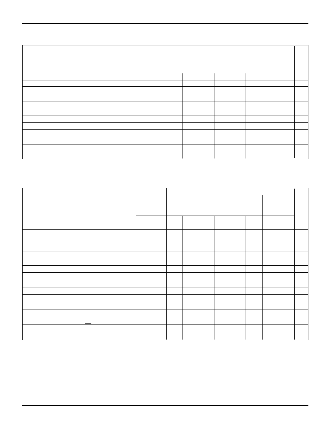
OPERATING CONDITIONS
(Commercial: VCC = 5.0V ± 10%, TA = 0°C to +70°C; Military: VCC = 5.0V ± 10%, TA = –55°C to +125°C)
Commercial
Commercial and Military(5)
Symbol
Parameter
IDT72401L45 IDT72401L35 IDT72401L25 IDT72401L15 IDT72401L10
IDT72403L45 IDT72403L35 IDT72403L25 IDT72403L15 IDT72403L10
Figure Min. Max. Min. Max. Min. Max. Min. Max. Min. Max. Unit
tSIH(1) Shift in HIGH Time
2
9
—
9
— 11 —
11 —
11 — ns
tSIL
Shift in LOW TIme
2
11 —
17 — 24 —
25 —
30 — ns
tIDS
Input Data Set-up
2
0
—
0
—
0
—
0
—
0
— ns
tIDH
Input Data Hold Time
2
13 — 15 — 20 —
30 — 40 — ns
tSOH(1) Shift Out HIGH Time
5
9
—
9
— 11 —
11 —
11 — ns
tSOL
Shift Out LOW Time
5
11 —
17 — 24 —
25 —
25 — ns
tMRW
Master Reset Pulse
8
20 —
25 — 25 —
25 —
30 — ns
tMRS
Master Reset Pulse to SI
8
10 —
10 — 10 —
25 —
35 — ns
tSIR
Data Set-up to IR
4
3
—
3
—
5
—
5
—
5
— ns
tHIR
Data Hold from IR
4
13 —
15 — 20 —
30 —
30 — ns
tSOR(4) Data Set-up to OR HIGH
7
0
—
0
—
0
—
0
—
0
— ns
AC ELECTRICAL CHARACTERISTICS
(Commercial: VCC = 5.0V ± 10%, TA = 0°C to +70°C; Military: VCC = 5.0V ± 10%, TA = –55°C to +125°C)
Commercial
Commercial and Military(5)
Symbol
Parameter
IDT72401L45
IDT72403L45
Figure Min. Max.
IDT72401L35
IDT72403L35
Min. Max.
IDT72401L25
IDT72403L25
Min. Max.
IDT72401L15
IDT72403L15
Min. Max.
fIN
Shift In Rate
2
— 45 — 35 — 25 — 15
IDT72401L10
IDT72403L10
Min. Max. Unit
— 10 M H z
tIRL(1) Shift In to Input Ready LOW
2
— 18 — 18 — 21 — 35 — 40 ns
tIRH(1) Shift In to Input Ready HIGH
2
— 18 — 20 — 28 — 40 — 45 ns
fOUT
Shift Out Rate
5
— 45 — 35 — 25 — 15 — 10 M H z
tORL(1) Shift Out to Output Ready LOW
5
— 18 — 18 — 19 — 35 — 40 ns
tORH(1) Shift Out to Output Ready HIGH
5
— 19 — 20 — 34 — 40 — 55 ns
tODH
Output Data Hold (Previous Word)
5
5
—
5
—
5
—
5
—
5
— ns
tODS
Output Data Shift (Next Word)
5
— 19 — 20 — 34 — 40 — 55 ns
tPT
Data Throughput or "Fall-Through"
4, 7 — 30 — 34 — 40 — 65 — 65 ns
tMRORL Master Reset to OR LOW
8
— 25 — 28 — 35 — 35 — 40 ns
tMRIRH Master Reset to IR HIGH
8
— 25 — 28 — 35 — 35 — 40 ns
tMRQ
tOOE(3)
tHZOE(3,4)
Master Reset to Data Output LOW
Output Valid from OE LOW
Output High-Z from OE HIGH
8
— 20 — 20 — 25 — 35 — 40 ns
9
— 12 — 15 — 20 — 30 — 35 ns
9
— 12 — 12 — 15 — 25 — 30 ns
tIPH(2,4) Input Ready Pulse HIGH
4
9
—
9
— 11 — 11 — 11 — ns
tOPH(2,4) Output Ready Pulse HIGH
7
9
—
9
— 11 — 11 — 11 — ns
NOTES:
1. Since the FIFO is a very high-speed device, care must be excercised in the design of the hardware and timing utilized within the design. Device grounding and decoupling
are crucial to correct operation as the FIFO will respond to very small glitches due to long reflective lines, high capacitances and/or poor supply decoupling and grounding.
A monolithic ceramic capacitor of 0.1µF directly between VCC and GND with very short lead length is recommended.
2. This parameter applies to FIFOs communicating with each other in a cascaded mode. IDT FIFOs are guaranteed to cascade with other IDT FIFOs of like speed grades.
3. IDT72403 only.
4. Guaranteed by design but not currently tested.
5. Military availability for IDT72403 is 10MHz, 35MHz. IDT72401 is available for all MHz.
3
Share Link: 