HV232GA(2001) Ver la hoja de datos (PDF) - Supertex Inc
Número de pieza
componentes Descripción
Fabricante
HV232GA
(Rev.:2001)
(Rev.:2001)
Supertex Inc

HV232GA Datasheet PDF : 10 Pages
| |||
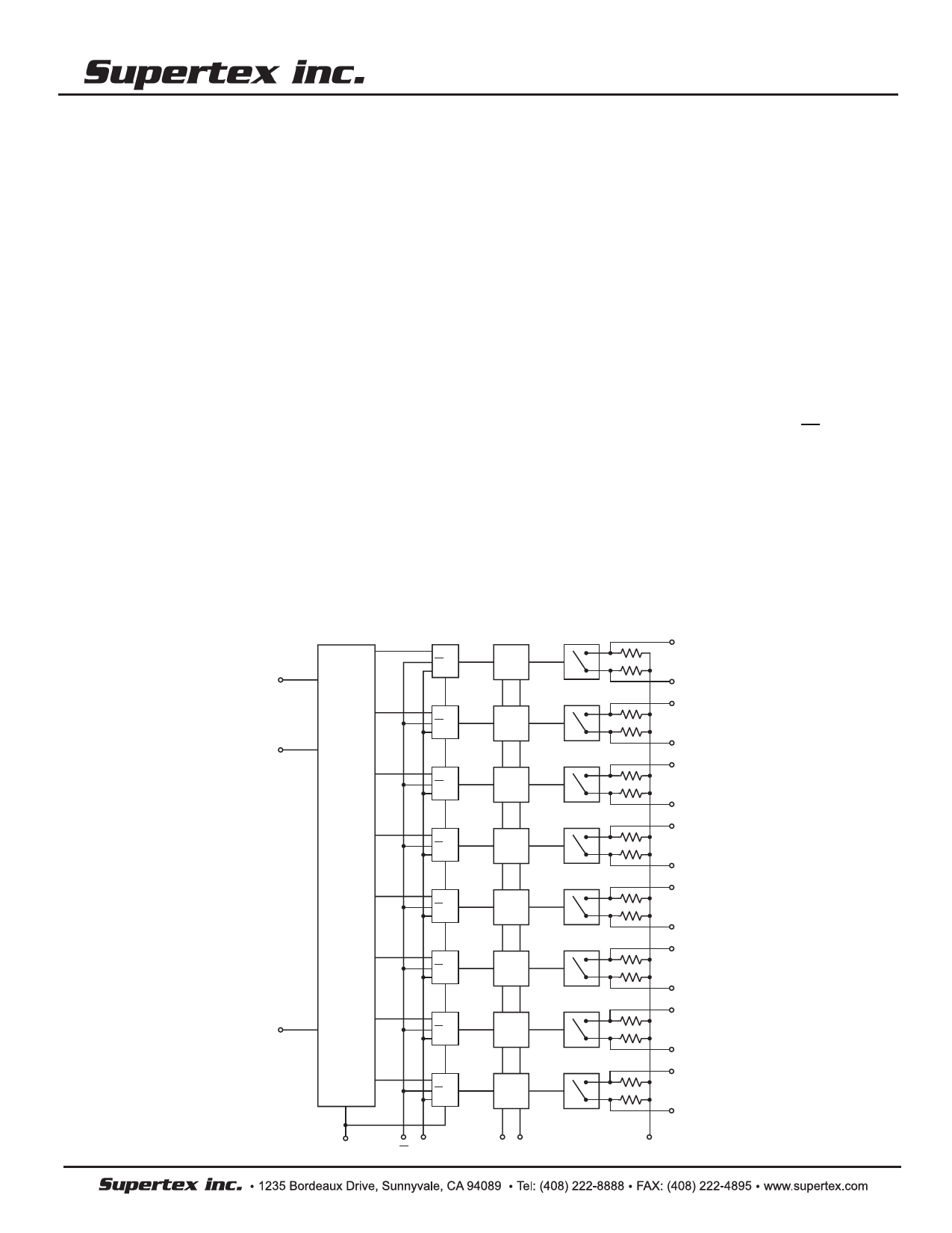
HV232
Low Charge Injection 8-Channel High Voltage
Analog Switch with Bleed Resistors
Ordering Information
VPP – VNN
200V
28-lead plastic
chip carrier
HV232PJ
Package Options
48-lead TQFP
µ-BGA
HV232FG
HV232GA
Die
HV232X
Features
❏ HVCMOS® technology for high performance
❏ Very low quiescent power dissipation – 10µA
❏ Output On-resistance typically 22 ohms
❏ Integrated bleed resistors on the outputs
❏ Low parasitic capacitances
❏ DC to 10MHz analog signal frequency
❏ -60dB typical output off isolation at 5MHz
❏ CMOS logic circuitry for low power
❏ Excellent noise immunity
❏ On-chip shift register, latch and clear logic circuitry
❏ Flexible high voltage supplies
❏ Surface mount package available
General Description
The Supertex HV232 is a low charge injection 8-channel high-
voltage analog switch integrated circuit (IC) with bleed resistors.
The device can be used in applications requiring high voltage
switching controlled by low voltage control signals, such as
ultrasound imaging and printers. The bleed resistors eliminate
voltage built up on capacitive loads such as piezoelectric trans-
ducers. Input data is shifted into an 8-bit shift register which can
then be retained in an 8-bit latch. To reduce any possible clock
feed-through noise, Latch Enable Bar (LE) should be left high
until all bits are clocked in. Using HVCMOS technology, this
switch combines high voltage bilateral DMOS switches and low
power CMOS logic to provide efficient control of high voltage
analog signals.
This IC is suitable for various combinations of high voltage
supplies, e.g., V /V : +50V/–150V, or +100V/–100V.
PP NN
Absolute Maximum Ratings*
VDD Logic power supply voltage
V - V Supply voltage
PP
NN
VPP Positive high voltage supply
VNN Negative high voltage supply
Logic input voltages
Analog Signal Range
Peak analog signal current/channel
-0.5V to +15V
220V
-0.5V to VNN +200V
+0.5V to -200V
-0.5V to VDD +0.3V
VNN to VPP
3.0A
Storage temperature
-65°C to +150°C
Power dissipation
µ-BGA
28-pin PLCC
48 lead TQFP
1.0W
1.2W
1.0W
* Absolute Maximum Ratings are those values beyond which damage to the
device may occur. Functional operation under these conditions is not implied.
Continuous operation of the device at the absolute rating level may affect
device reliability.
10/31/01
Supertex Inc. does not recommend the use of its products in life support applications and will not knowingly sell its products for use in such applications unless it receives an adequate "products liability
indemnification insurance agreement." Supertex does not assume responsibility for use of devices described and limits its liability to the replacement of devices determined to be defective due to
workmanship. No responsibility is assumed for possible omissions or inaccuracies. Circuitry and specifications are subject to change without notice. For the latest product specifications, refer to the
Supertex website: http://www.supertex.com. For complete liability information on all Supertex prod1ucts, refer to the most current databook or to the Legal/Disclaimer page on the Supertex website.
Share Link: