28F008C3 Ver la hoja de datos (PDF) - Intel
Número de pieza
componentes Descripción
Fabricante
28F008C3 Datasheet PDF : 59 Pages
| |||
E
3 VOLT ADVANCED+ BOOT BLOCK
1.0 INTRODUCTION
This document contains the specifications for the
3 Volt Advanced+ Boot Block flash memory family.
These flash memories add features which can be
used to enhance the security of systems: instant
block locking and a protection register.
Throughout this document, the term “2.7 V” refers
to the full voltage range 2.7 V–3.6 V (except where
noted otherwise) and “VPP = 12 V” refers to 12 V
±5%. Sections 1 and 2 provide an overview of the
flash memory family including applications, pinouts,
pin descriptions and memory organization. Section
3 describes the operation of these products. Finally,
Section 4 contains the operating specifications.
1.1 3 Volt Advanced+ Boot Block
Flash Memory Enhancements
The 3 Volt Advanced+ Boot Block flash memory
features:
• Zero-latency, flexible block locking
• 128-bit Protection Register
• Simple system implementation for 12 V
production programming with 2.7 V in-field
programming
• Ultra-low power operation at 2.7 V
• Minimum 100,000 block erase cycles
• Common Flash Interface for software query of
device specs and features
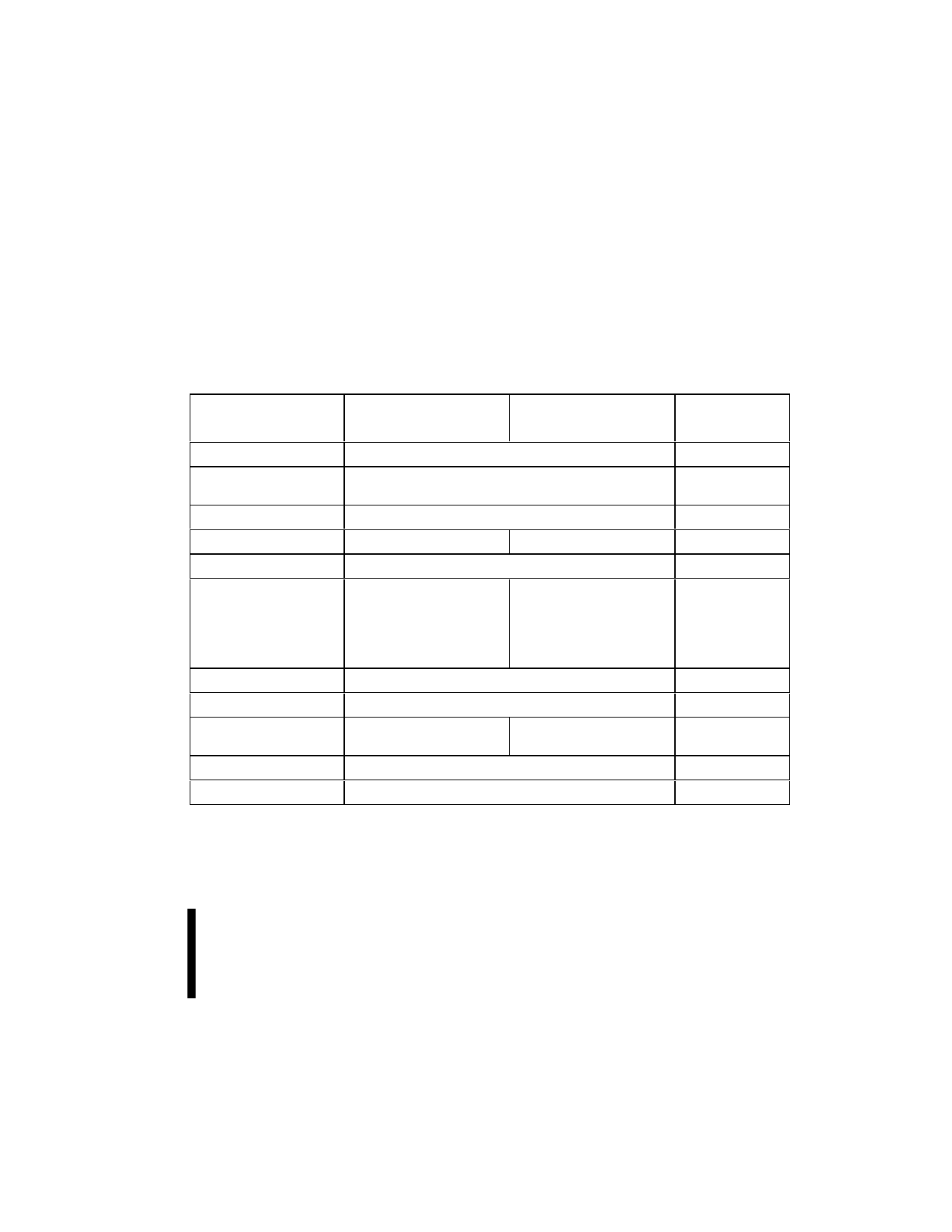
Table 1. 3 Volt Advanced+ Boot Block Feature Summary
Feature
8 M(2)
16 M
32 M(1)
8 M(2)
16 M
32 M
Reference
VCC Operating Voltage
2.7 V – 3.6 V
Table 8
VPP Voltage
Provides complete write protection with
optional 12V Fast Programming
Table 8
VCCQ I/O Voltage
2.7 V– 3.6 V
Note 3
Bus Width
8-bit
16-bit
Table 2
Speed (ns)
90, 110 @ 2.7 V and 80, 100 @ 3.0 V
Table 11
Blocking (top or bottom)
8 x 8-Kbyte parameter
4-Mb: 7 x 64-Kbyte main
8-Mb: 15 x 64-Kbyte main
16-Mb: 31 x 64-Kbyte main
32-Mb: 63 x 64-Kbyte main
8 x 4-Kword parameter
4-Mb: 7 x 32-Kword main 8-
Mb: 15 x 32-Kword main
16-Mb: 31 x 32-Kword main
32-Mb: 63 x 32-Kword main
Section 2.2
Appendix E and F
Operating Temperature
Extended: –40 °C to +85 °C
Table 8
Program/Erase Cycling
100,000 cycles
Table 8
Packages
40-Lead TSOP(1)
48-Ball µBGA* CSP(2)
48-Lead TSOP
48-Ball µBGA* CSP(2)
Figures 1, 2, 3,
and 4
Block Locking
Flexible locking of any block with zero latency
Section 3.3
Protection Register
64-bit unique device number, 64-bit user programmable Section 3.4
NOTES:
1. 32-Mbit density not available in 40-lead TSOP.
2. 8-Mbit density not available in µBGA* CSP.
3. VCCQ operation at 1.65 V — 2.5 V available upon request.
PRODUCT PREVIEW
5
Share Link: 